hi team,
my customer is using DRV8350H and below are some problems that need your help:
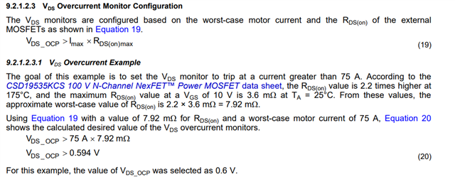
1. the OCP current limit: do we have a specific formula how to calculate the current limit between VDS?
2. Can DRV8350 work with AMC1306?
3. the datasheet shows that DRV8350 supports 100% PWM. Could u kindly help to explain the principle? because when the PWM is up to 100%, when will the charge pump of high side be charged?
4. Is there any error in figure 20 about the VCC? One VCC is the output pin of the chip, one is the pull up voltage of nfault.thanks!