This thread has been locked.

If you have a related question, please click the "Ask a related question" button in the top right corner. The newly created question will be automatically linked to this question.

DRV8889-Q1: The first movement of the motor after powering up the current output is particularly high resulting in a very loud noise.

Part Number: DRV8889-Q1

Hello TI

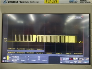
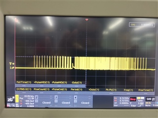
When I use the same configuration input to DRV8889-Q1, including SPI register configuration, VREF (35%), STEP transmit frequency configuration, etc.

There will be a very noisy motor caused by the first movement of the motor after the first power up of the software outputting 2.5 times more current.

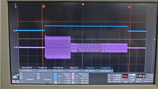
In the figure below, there are five movements, and the VREF (blue line) input is the same throughout the whole process. The amplitude of AOUT1 in the first movement is nearly twice as much as in the second movement, but the frequency of the first movement, the second movement, and the last movement are the same.

  • Output trend of AOUT voltage at the time of noise generation

    Output of AOUT voltage without noise generation

  • Hello,

    It appears you have enabled the outputs permanently or enabled prior to configuring the TRQ_DAC register to 35% current. When the device is powered on with DRVOFF pin set to 1 the driver will output A & B HOME position currents with TRQ_DAC set to 100% its default value. This will be 71% of the current set by the VREF voltage with TRQ_DAC at 100%. For example if VREF = 3.3V the peak current would be 1.5A. 71% of this value would be output on both windings, about 1A.

    If you have DRVOFF pin permanently enabled and do not desire this behavior there are couple of solutions to consider.

    1. Control DRVOFF pin with the ECU and keep it HIGH by default. DRVOFF can be enabled after writing the desired IFS current (full-scale) to the TRQ_DAC.

    2. Set the VREF value to the maximum IFS desired in the application. For example if you would want 500mA IFS VREF should be 1.1V. This can be set using two resistors based potential divider like described in the datasheet. 

    3. Use the 'A' variant of this device, DRV8889A-Q1. This is a drop in device both from HW and SW except for a few differences mentioned in the DRV8889-Q1 datasheet. Primarily, in this device the DIS_OUT bit is 1b by default. So, after power on you can first write to TRQ_DAC register to set 35% of the current and then write DIS_OUT to 0b to enable the outputs.

    In your setup the first movement seems to be with TRQ_DAC not correctly set. I have marked a transition in IFS with an arrow TRQ_DAC. Was the TRQ_DAC written with the value at that point?

    What are the observed spikes I marked with red arrows in the VREF (blue trace)? Thanks.


    Regards, Murugavel


  • Hello Murugavel4637,

    Verify that DRVOFF pin set to 0 before writing TRQ_DAC.
    And the cause has been found, it seems that it takes some time to write to the DRV8889-Q1 registers using SPI and then read back the correct value, what is the approximate time required for this?

    I delayed one more task cycle (10ms for our project) before sending the pulse, and everything is fine, and the TRQ_DAC read is correct using SPI!

  • Hello,

    Yes we have specification for SPI communication ready time after power up or wake up from sleep. Please see below. Thanks.

    Regards, Murugavel