Other Parts Discussed in Thread: DRV8210, DRV8212, DRV8210P, DRV8212P, DRV8801A-Q1, DRV8876-Q1, DRV8262
Tool/software:
Hello Expert,
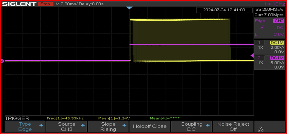
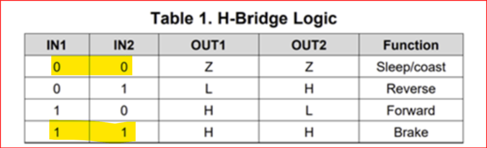
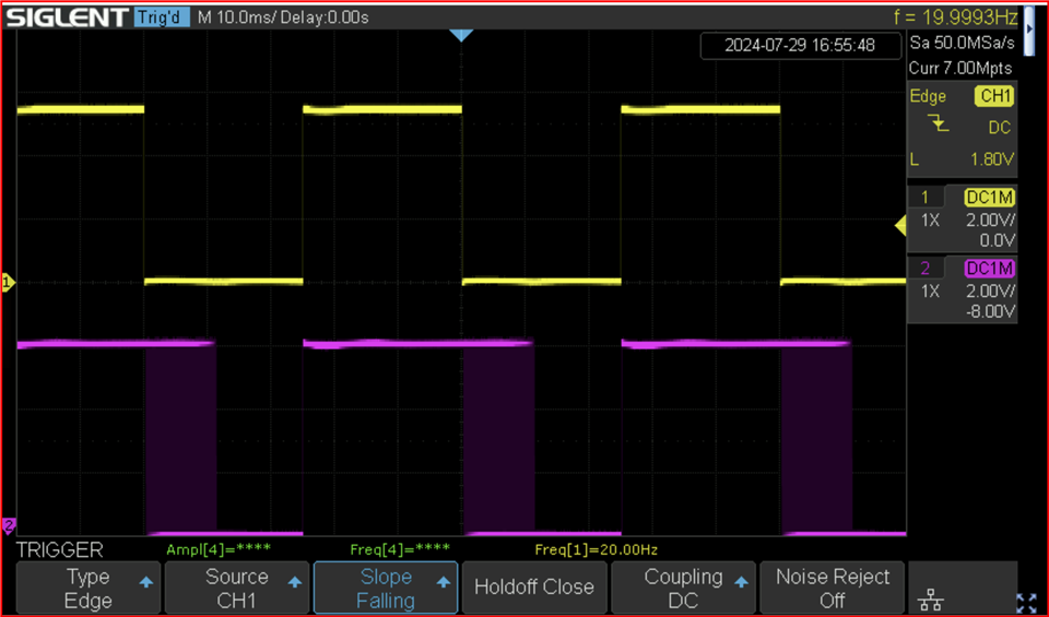
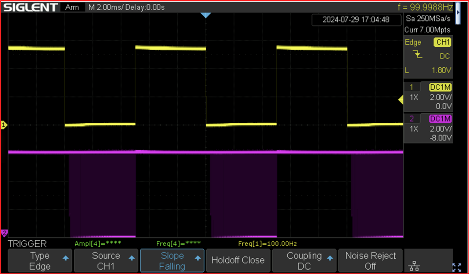
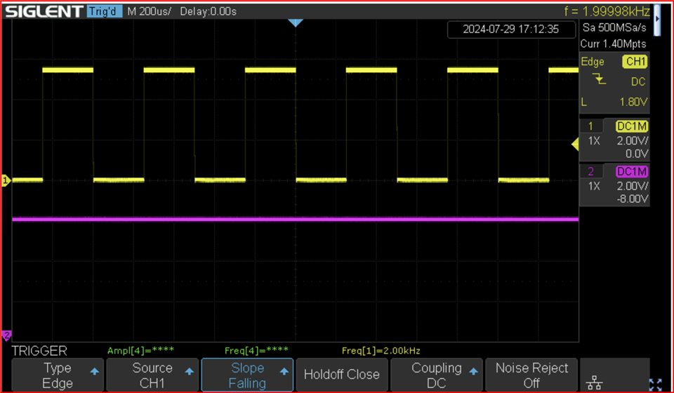
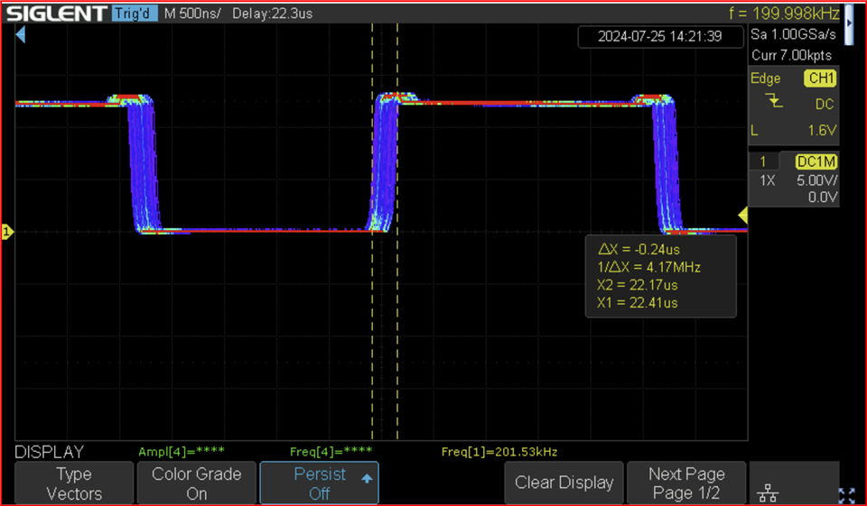
Could you please tell me maximum input frequency?
We are planning to use 20Hz to 20kHz signal.
But voltage regulation Internal PWM frequency is 44.5kHz
So, I suppose the input signal frequency is limited and it is depends on Voltage regulation setting.
Best regards,
Kazuki Kuramochi