This thread has been locked.

If you have a related question, please click the "Ask a related question" button in the top right corner. The newly created question will be automatically linked to this question.

DRV8301 : Trickle Charge Circuitry and Internal Handshake

Other Parts Discussed in Thread: DRV8301

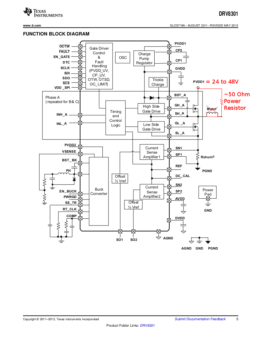
I'm using the DRV8301 to drive a two-phase buck-converter to charge a 24V battery.  In this situation, the half-bridge outputs have a non-zero voltage (about 24V) present on them before the DRV8301 starts driving the FET gates.    

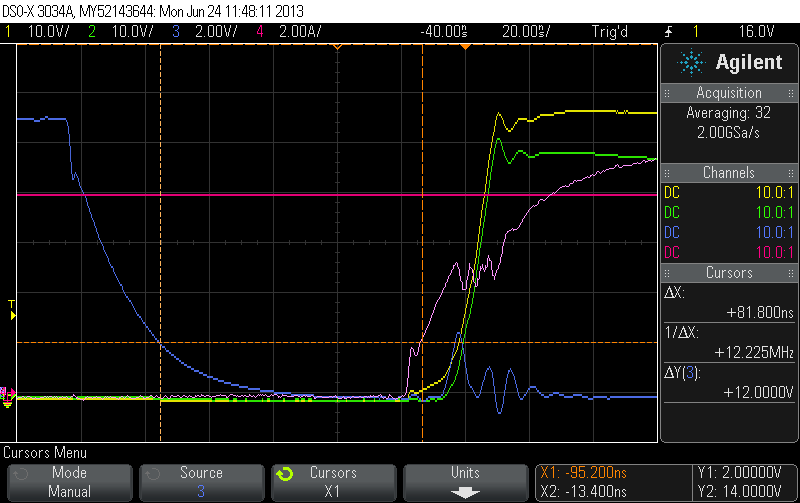
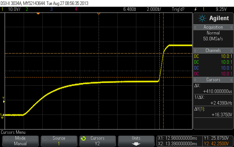
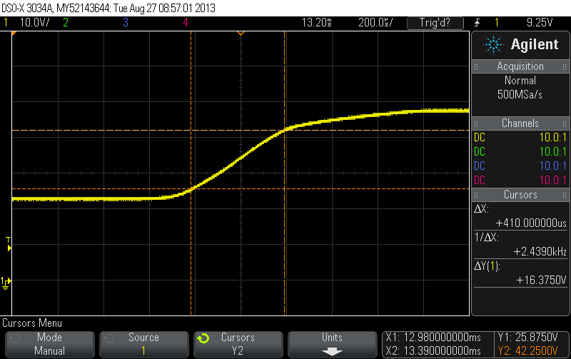
The presence of 24V almost guarantees that the output bootstrap capacitors will start with no charge.    If the half-bridge output is 24V, the BST_x pins will have higher voltage on them than the GVDD voltage of ~10V.    I believe this causes a small reverse leakage current through the internal bootstrap diode which discharges the bootstrap capacitor to have zero or slightly negative voltage.

At first I hoped the DRV8301 trickle charge circuitry would counteract any leakage on the bootstrap capacitor.  However, the trickle charge circuitry only seems to operate when the INH_x input is high.    This makes sense, since the datasheet only specifies the trickle charge circuitry allows 100% duty operation, not that it pre-charges the bootstrap cap:

"Bootstraps are used in highside FETs of three-phase pre-gate driver.  Trickle charge circuitry is used to replenish current leakage from bootstrap cap and support 100% duty cycle operation."

It would be nice if the trickle charging was operating all the time and the bootstrap cap would automatically be charged a few milliseconds  DRV8301 gate enable signal was asserted.  

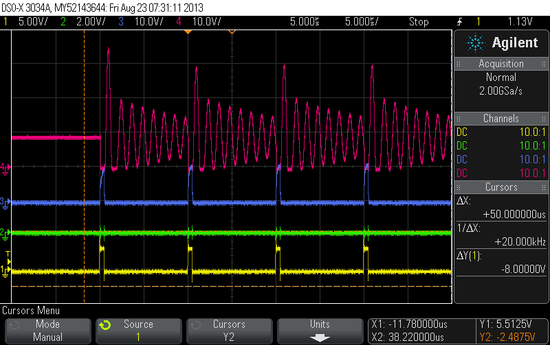
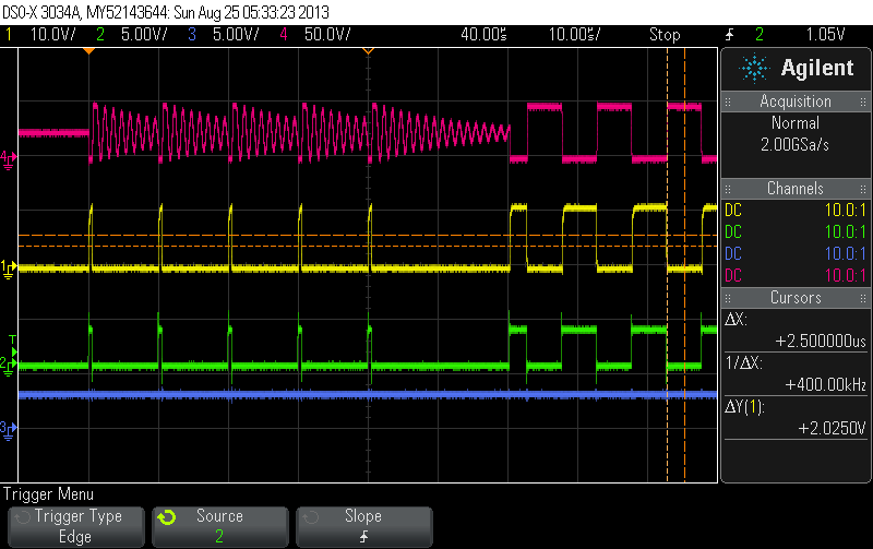
With most bootstrap-based gate drivers without trickle charging, you need to pulse the lowside FET on for a few short bursts before enabling the normal PWM operation.   These short on pulses on the lowside FET will drive output voltage to zero and charge the bootstrap capacitor through the bootstrap diode.    The short pulses also slowly pump up the bootstrap capacitor instead bringing it to full voltage all at once.

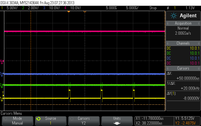
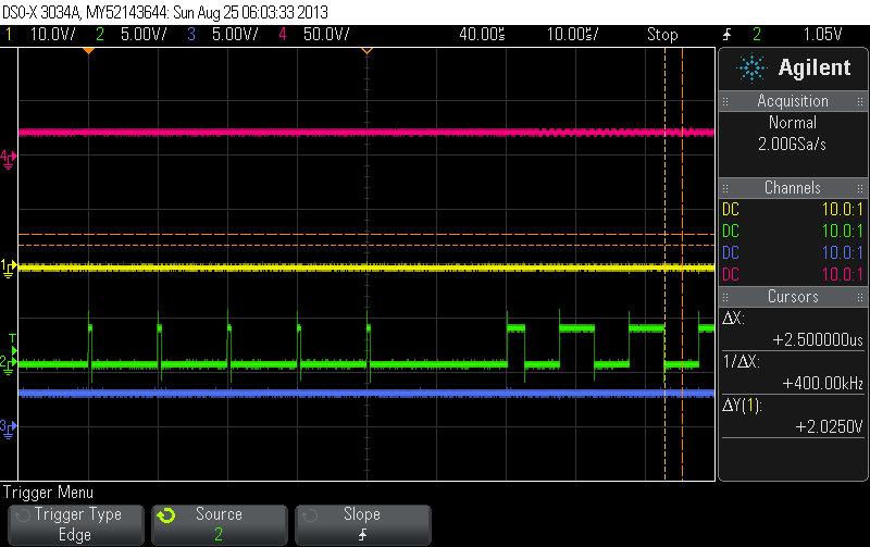
In my case the short pumping pulses work...  but only sometimes.    Much of the time, the DRV8301 totally ignores the low-side gate pulse (the input get the signal, but the LS gate output does not do anything).  When the lowside gate pulse is ignored, it is always ignored, no mater how long it is run.   This is not caused by a FAULT or OCTW.   I tie both signals together and never not see it assert low when DRV8301 is ignoring low-side pulses.    However, I do get a OC fault on the high-side FET the first time the highside input is asserted.   I believe this is because there is no voltage on the bootstrap capacitor and no voltage voltage to HS FET Vgs.   The FET is not turned on and the OC detects this as a high-side MOSFET is over current.

When the DRV8301 does let the low side pulses through, it does so immediately.  I've never see it drop the first few  drop the first few pulses and then start working later.   However, when the pulses do go through,  they usually work again if I reset the DRV8301 and restart soon after.  

I have the software write and verify the DRV8301 control registers before sending the first PWM signal, so I'm sure the DRV8301 is powered-up and operating.   I also poll the GVDD_UV status bit through the SPI, so I know the GVDD is happy before starting up.   I've also tried a different board so it is unlikely that the problem is caused by a damaged DRV8301.    

If I don't have an external 24V on the half-bridge before starting, the low-side pulses always go through without issue.   However, there will always be an external 24V on the half-bridge outputs in the real system, so this is not a fix.

I'm guessing there is something wrong with the handshaking between the lowside and highside signals when there is no voltage on the bootstrap cap.    Is it possible to get a description on how the handshaking operates, or a confirmation that this might be an issue?   

I would also appreciate any suggestions on how to trick the trickle charge circuitry into the pre-charging the bootstrap capacitor.   I am considering putting the DRV8301 in OC protect mode,  pulsing the high-side PWM, and then waiting for OCTW/FAULT to stop occurring before switching to a full PWM.   This is an ugly hack, but might work.

  • Hi Derek,

    We will have to confirm how the trickle charge works and get back to you. While we are checking can you answer a few questions?

    Which PWM mode are you using (6 or 3 independent inputs, refer to Table 7 of the datasheet)? If the default, are you driving the INL_x signal high while holding the INH_x signal low to charge the bootstrap cap? What is the deadtime used?

    Do you have a spare half bridge available in your application?

  • I'm using 6-input mode.   When the pumping the bootstrap cap, I keep the high-side inputs low the entire time, and have a short PWM pulse (0.5us) on the lowside.   I've hooked up probes to the gate driver inputs to make sure the code wasn't doing anything unexpected.

    When the device does work (when 24V is not present at start-up) the 0.5us pulse is enough to charge the bootstrap in 2-3 pulses.  

    Currently there is no deadtime inserting by the hardware.   Earlier I tuned the deadtime against the switching waveform, and  found the 50ns minimum deadtime inserted by the DRV8301 itself in more than enough.  I'm attaching the gate drive waveform:

    • 48V supply, 4Amp load per half-bridge
    • 0.7Amp gate drive setting
    • 0 Ohm deadtime resistor on DRV8301
    • no deadtime injection by uC
    • Yellow : highside FET gate input (10V/div)
    • Green : highside FET source (output voltage) (10V/div)
    • Pink : Math (Yellow-Green) = HS FET Vgs  (5V/div)
    • Blue : Low side FET gate input 
    • Red : Current sense on load (shared between two half-bridge)


  • Hi Derek,

    As you suspected, the trickle charge circuit does not operate when the GH_x is low. The internal diode shown in the block diagram of the datasheet handles charging the bootstrap cap. It is expected that the SH_x signal will be cycled low initially to charge the bootstrap cap.

    When 24V is present and you pulse the low gate input for .5us, does SH_x drop to less 1V? If not, the bootstrap cap is not being fully charged. You may have to increase the pulse on GL_x to achieve this.

    Do you have unused GH_x, SH_x, BST_x, and GL_x, and other pins? If so, what pins are unused on your device? We are looking into potential tricks but it may require a few extra components.

  • When the DRV8301 does respond to the PWM pulse on the INL_x signal the SH_x drops to nearly zero volts and charges the bootstrap cap.   Once the bootstrap has some amount of charge on it, everything works as expected from that point forward.

    The problem is when I assert INL_x high, the DRV8301 does not always drive GL_x high.    This seems to occur when the voltage in the SH_x pins starts at a voltage above 18V.   While not perfectly consistent  the problem occurs > 90% of the time.    When the SH_x starts out with a lower voltage, the DRV8301 always passes through the INL_x signal to the GL_x gate output.  

    I'm attaching two screen captures that were taken of  the DRV8301.  

    In the first capture, the initial output voltage was 9V and the DRV8301 worked properly.   The microcontroller sends short pulses into the INL_x pin (Yellow), while leaving the INH_x (Green) pin low.   When the DRV8301 sees INL_x go high, it then drives lowside gate output (Blue) high.   The half-bridge output (Red) is pulled low while lowside gate output is high.  When gate output goes low again the half-bridge output is high-Z and the inductor and output capacitor causes ringing of the voltage signal.   

    In the next screen capture the initial output is 24V and the DRV8301 does not work.   The low side gate input (SL_x) is pulsed high, but nothing shows up on the gate output (GL_x).   There is not much to see because the DRV830 is just not working.

    I've also tried putting a 1MOhm pull-up from SH_x to my 48V supply.    I also put a zener in parallel with bootstrap cap to prevent it from overcharging.    In this case the the lowside pulsing works even when the output voltage starts at 24V. 

    Here's the most clear description of the problem:

    When SH_x starts > 18V, AND the high-side bootstrap capacitor is not charged (SH_x == BST_x),  then the DRV8301 will not allow lowside gate (GL_x) to go high.   

    Since there is no FAULT occurring, I'm guessing something else is going wrong with the DRV8301.    AFAIK, the DRV8301 has some sort of hand-shaking mechanism to prevent the lowside MOSFET from being turned on when the highside MOSFET is also on.    I believe this handshaking mechanism might not work correctly when the SH_x voltage starts high AND there is no charge on the bootstrap capacitors (ie SH_x = BST_x).    

  • Hi Derek,

    I think you have narrowed down the issue. Please refer to pages 14, 15 and 21 of the datasheet. The important sections are "Over-Current Protection (OCP) and Reporting" and "Over Current Adjustment".

    What are the settings in the SPI register 0x02 for OC_MODE and OC_ADJ_SET?
       If default, then please look at the OCTW pin when the low side gate signal is not operating. If this signal is going low during the time you are attempting to turn on the low side FET,  the VDS across the low side FET is higher than the limit. Please look at the VDS across the low side FET. If above .4V +/- 20%, this can cause the gate driver to turn off.
       To correct this, there are a few options. The best one is to change the OC_ADJ_SET value based on the RDSon of your FET and the current limit you want. The second option is to change the OC_MODE to either Report only or OC protection disabled. This second option should be used for debug only. If you don't write to the registers, changing to a lower RDSon FET is third option.

    Can you provide the RDSon of your low side FET, and how much current is going through it when the problem is seen?


  • The OC_MODE is set to 1 (latched shutdown).  The OC_ADJ_SET is set to 8 (1.75Volts).    After writing the control register values, I read them back to verify the write worked correctly. 

    There is no current going through the lowside FET when the problem occurs.   The FAULT or OCTW pins are not asserted low while low-side gate refuses to operate.   This is why I'm leaning toward an issue with the hand-shaking mechanism.   

    At this point, I know that partially charging the bootstrap capacitor will fix my problem.   Ideally I would find a way to get the trickle charger to operate without having the DRV8301 attempt to drive the high-side FET gate.  

    The datasheet is short on details about how the hand-shaking mechanism works.   However, I'm guessing that it will prevent both the high-side and low-side gates from turning high at the same time.   If I drove both the INL_x and INH_x inputs high at the same time what would occur?

    1. Would neither the high-side and low-side gates turn-on?   In this case would bootstrap trickle charger still operate?
    2. Would the low-side (or high-side) take priority, turning on the low-side and blocking the high-side?
    3. Something else?
  • Hi Derek,

    Please confirm the OC_ADJ_SET value. "8" is .175V, not 1.75V.

    I was informed that low values of OC_ADJ_SET may cause this. As an experiment, please set the OC_MODE to 3 (disabled). This will provide additional debug information. If this works, then please set the OC_ADJ_SET to 31 and OC_MODE back to 1. OC_ADJ_SET can then be reduced until a reasonable value is set.

    If this does not work, can you provide schematics and layout in their native program? This may help us determine if there is a board problem that is appearing as the voltage increases. If you do not want to post them here, we can arrange an alternate path.

  • Sorry, 1.75 was a typo 0.175 is correct.   If I start with low external voltage, (SH_x < 16V),  I can run 8 amps without a fault.   Even with the lowest possible setting I can handle ~4Amps with a fault.   

    When a fault does occur, the code reads the status registers.  I've definitely had OC faults before, and they always triggered by having to high of a current or not having the bootstrap capacitor charged.   This is the reason I believe the DRV8301 fault output and firmware is working correctly.   

    With the problem I am having,  I do not see the fault being asserted.   Are you suggesting that the fault flag might not be set  at start-up when an over current condition flag is set?

    I'll try your your suggestion, and see what happens.   I can't post the design to the forum, I'll need an alternate option.

  • Hi Derek,

    At this point, I don't want to rule out any possibility. I cannot explain why fault does not assert with the settings you have. We hope that disabling the OC limit will allow you to continue, while we determine if there is a reason you are not seeing fault assert.

    The alternate path has been set up.

  • Scope Probe Setup:

    • Blue : FAULT and OCTW (tied together)  (5v/div)

    • Green : INL_x (5V/div)

    • Yellow : GL_x (10V/div)

    • Red : Half-Bridge Output Voltage (also SH_x) (50V/div)


    The following captures show the DRV8301 start-up sequence.   First, the low side gate is given five short pulses to pre-charge the bootstrap capacitor.   Then a full PWM is given to both highside and lowside inputs.  The PWM is about 50% duty.   The supply voltage is 48V, the output voltage starts at 24V.


    The first capture shows the DRV8301 working correctly.   In this case, the bootstrap capacitor is pre-charged using a 1MOhm resistor connected to the 48V supply.  The initial voltage on the bootstrap capacitor is about 8.2V.   There is a 13V zener diode in parallel with the bootstrap capacitor to prevent over-charging of capacitor.   However, even without the zener, the capacitor usually only charges to 8-9V.  This is possibly due to leakage through the internal bootstrap diode.


    The only change in the the second capture, is that the 1MOhm pullup resistors are removed.  The microcontroller firmware was not changed or reprogrammed.   In both the first and second captures, the DRV8301 is set to OC latched shutdown mode.  

    In the 2nd capture, the initial bootstrap capacitor voltage is -0.020V (as measured by DMM).    In the capture, the signal on the lowside INL_x input is not translated to the GL_x output.


    In the 3rd capture, the 1MOhm pull-ups are removed and the DRV8301 is set to OC protection disabled mode.   After a few full PWM cycles, the microcontroller will disable the PWM and re-read all the control and status registers to make sure the settings have not changed:

    • CTRL1: 0x0231

    • CTRL2: 0x0004

    • STAT1: 0x0000

    • STAT2: 0x0001


    Finally, I also ran the DRV8301 in report only mode, it produced the same result as 2nd and 3rd captures.


  • Hi Derek,

    Thanks for the additional info. We are evaluating this information now.

    Can you send the information requested through the alternate path? This will allow duplication of your setup and procedures as accurately as possible.

    Also, what is the PVDD ramp rate when the device works and when it does not? Is it possible that the maximum rate of 1V/us is being violated?

  • This the turn-on profile of the PVDD1 power rail.  The max ramp rate is 0.04V/uc.   


    A more zoomed in version on faster second ramp /


  • I think the easiest way to get a reproduction is by modifying a DRV8301 dev board :

    Connecting the output to the supply voltage with a ~50 Ohm power resistor will pull the initial SH_x voltage higher than 18V.   Even if the DRV8301 does drive the output, there will only be less 2Amps of current.   Unfortunately, I do not have a DRV8301 dev board, so I can't guarantee this will reproduce the issue.   

  • Hi everyone,

    I have exactly the same problem trying to drive two dc motors having one of the poles connected to the positive supply.

    The problem seems to be solved connecting a 1M resistor from gate to source of the high side mosfets, but I don't know why.

    Have anyone analyzed the matter further?

  • Hello Simone,

    This thread seems to have gone stale. Please create a new thread explaining your issue for better support. Thank you very much.