Hi,
I'm currently having problems reading from my DRV8711 chip. The writes seem to work fine since my application (which only needs to write to the driver) works as intended. I'm now trying to read the registers from the driver, but I can't seem to make it work as told by the datasheet.
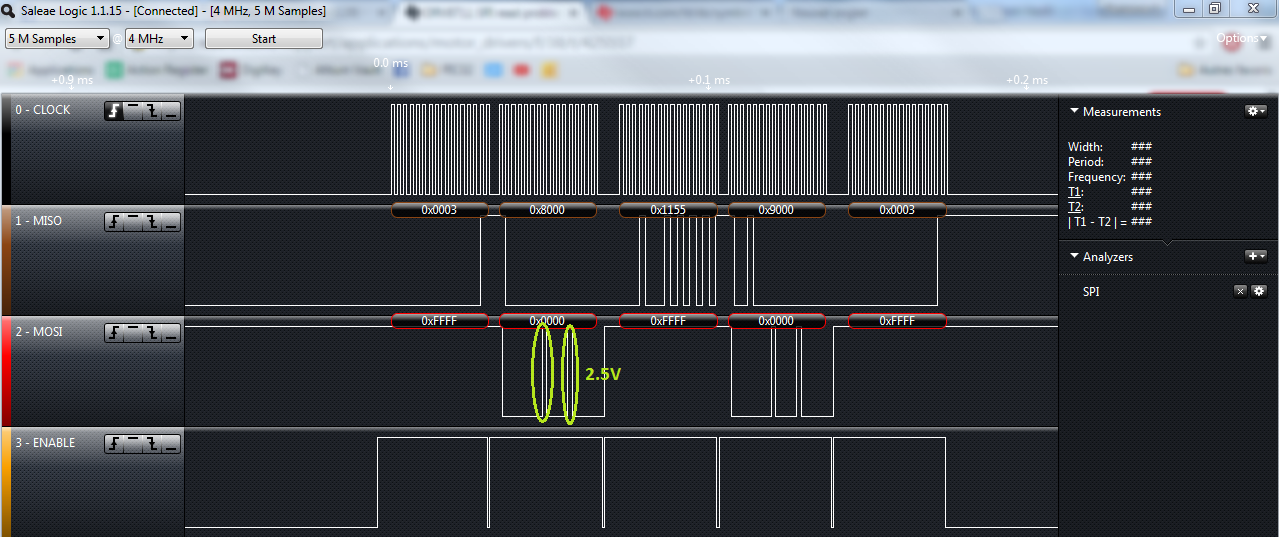
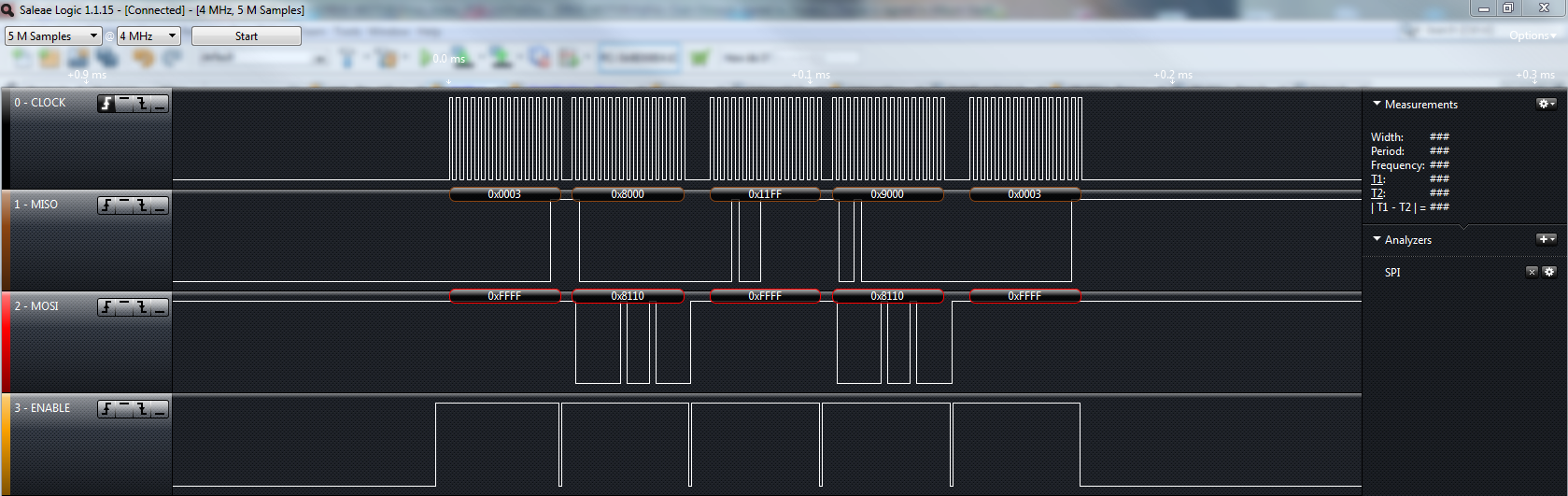
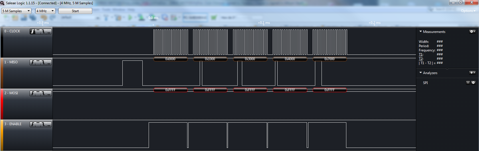
I looked at the traffic on my SPI line between my microcontroller and the driver and it looks fine. First, I write 0x003 to the CRTL register (0x0003) and then I read from the same register (0x8000). According to the datasheet, the data should be outputed from the drive after the first byte (0x8) and I should read 0x003 from the line. Then, for the sake of testing, I write to the TORQUE register (0x11FF) and read from it (0x9000). I should then be able to read (0x1FF) from the line. I finish with a write to the CTRL register (0x0003).
However, the data on the line is nothing like I expected. I analyzed the data with a Saelae and here is a screenshot of what it looks like (MISO is data out from the master and MOSI is data in to the master) :
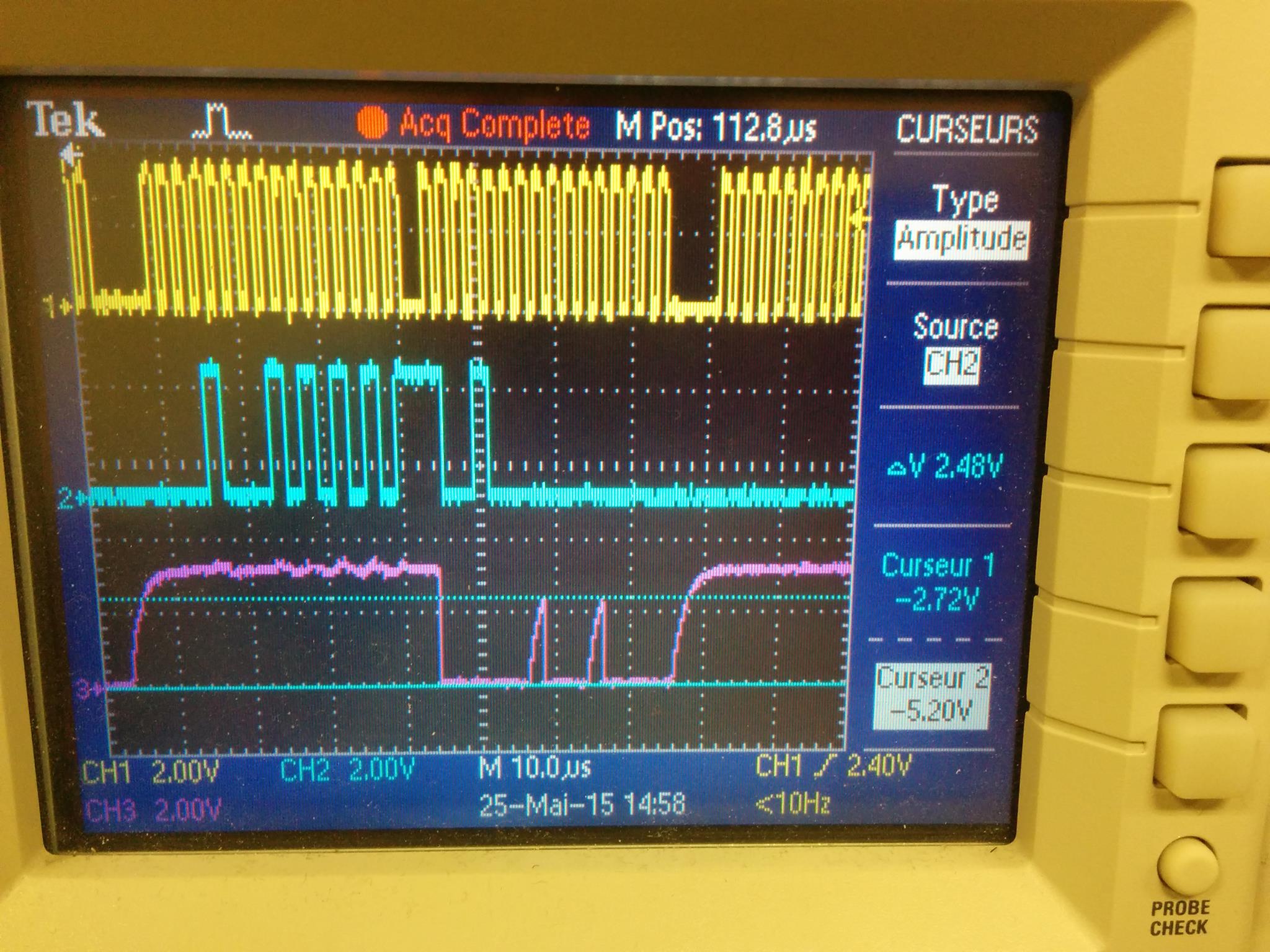
The master clock is set at 500 kHz and on 16 bits/word transmission. The pin RESET is set at zero (0) at my initialization and the pin SLEEPn at one (1). Am I missing something? Here is a picture of what my initialization looks like :
Thank you for your help and please let me know if you need more information.
Fred