Hi There,
I had the same problem as a previously solved in an older post but in the solved post there was no description of what was done to solve the issue.
Essentially I am writing to the DRV registers to set them up and then reading the information back but i only read 0x0000 when the enable pin is low and 0xFFFF when its high. All registeres seem to respond with 0x0000. I do not know if its because my control words are setup incorrectly, if its an SPI library quirk, if its hardware related or if its pure stupidity.
I am using the Mbed SPI libraries. with the SPI set to 1Mhz clock, 16 bit words, clock polarity : clock active low, clock in phase with data. I also wait 1 -2 us between each control word (raising and lowering nCSC)
1) Is the ENABLE pin set to a logic high?
Yes
2) How fast are you running the SPI?
1 Mhz
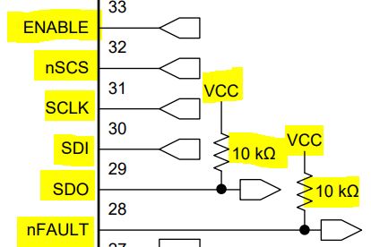
3) What is the pullup value on SDO?I
t was 100k then changed to 10k, not difference noticed.
4) Can you capture SDO with a scope instead of a logic analyzer?
Not yet will try tho. Currently using a Nucleo F746ZG and Analyzer2Go to analyze the bit on the SPI pins.
I can post a snap shot of the Analyzer data if you would like to see that. and I have attached my code at the below for your interest.
#include "mbed.h"
#include "DRV8323.h"
#include "stdbool.h"
#include "stdint.h"
//#include "stm32f4xx_hal.h"
DigitalOut myLED1(LED1);
DigitalOut myLED2(LED2);
DigitalOut myLED3(LED3);
Serial pc(USBTX, USBRX); // setup USB interface to host terminal
//SPI device(SPI_MOSI, SPI_MISO, SPI_SCK);
DigitalOut SSEL1(PE_4);//SSEL1 or CS1
//DigitalOut SSEL2(PE_7);//SSEL2 or CS2
SPI DRV8323_SPI(PE_6, PE_5, PE_2);
//default values for the DRV8323 registers
uint16_t DRV8323regDrvCtrl =
0 << 9 | //DIS_CPUV
1 << 8 | //DIS_GDF
0 << 7 | //OTW_REP
0 << 5 | //PWM_MODE
0 << 4 | //1PWM_COM
0 << 3 | //1PWM_DIR
0 << 2 | //COAST
0 << 1 | //BRAKE
0; //CLR_FLT
uint16_t DRV8323regGateDrvHS =
3 << 8 | //LOCK
11 << 4 | //IDRIVEP_HS
15; //IDRIVEN_HS
uint16_t DRV8323regGateDrvLS =
1 << 10 | //CBC
2 << 8 | //TDRIVE
15 << 4 | //IDRIVEP_LS
15; //IDRIVEN_LS
uint16_t DRV8323regOcpCtrl =
0 << 10 | //TRETRY
1 << 8 | //DEAD_TIME
1 << 6 | //OCP_MODE
2 << 4 | //OCP_DEG
0; //VDS_LVL
uint16_t DRV8323regCsaCtrl =
1 << 10 | //CSA_FET
1 << 9 | //VREF_DIV
0 << 8 | //LS_REF
2 << 6 | //CSA_GAIN
0 << 5 | //DIS_SEN
0 << 4 | //CSA_CAL_A
0 << 3 | //CCSA_CAL_B
0 << 2 | //CCSA_CAL_C
3; //CSEN_LVL
void DRV8323_initiate_SPI(void);
uint16_t DRV8323_readSpi(uint8_t regAdr);
void DRV8323_writeSpi(uint8_t regAdr, uint16_t regVal);
void DRV8323_setupSpi(void);
DigitalIn mybutton(USER_BUTTON);
int main()
{
volatile uint16_t temp;
myLED1= 1;
myLED2= 0;
myLED3= 1;
DRV8323_initiate_SPI();
wait_us(10);
while(1) {
if (mybutton == 1) { // Button is pressed
myLED3= !myLED3;
DRV8323_setupSpi();
//wait(0.2); // 200 ms
}
//DRV8323_writeSpi(ADR_DRV_CTRL, DRV8323regDrvCtrl);
wait_us(1);
temp = DRV8323_readSpi(ADR_FAULT_STAT);
pc.printf("WHOAMI register = 0x%X\n", temp);
myLED1 = !myLED1;
myLED2 = !myLED2;
wait_us(50);
}
}
void DRV8323_initiate_SPI()
{
SSEL1 = 1;
// Setup the spi for bit data, high steady state clock,
// second edge capture, with a 1MHz clock rate
DRV8323_SPI.format(16,3);
DRV8323_SPI.frequency(1000000);
}
uint16_t DRV8323_readSpi(uint8_t regAdr)
{
uint16_t controlword = 0x8000 | ((regAdr & 0x7) << 11); //MSbit =1 for read, address is 3 bits (MSbit is always 0), data is 11 bits
// Select the DRV device by setting chip SSEL1 = 0 low
SSEL1 = 1;
wait_us(1);
SSEL1 = 0;
uint16_t whoami = DRV8323_SPI.write(controlword);
wait_us(2);
SSEL1 = 1;
DRV8323_SPI.clear_transfer_buffer();
return(whoami);
}
void DRV8323_writeSpi(uint8_t regAdr, uint16_t regVal)
{
uint16_t controlword = (regAdr & 0x7) << 11 | (regVal & 0x7ff); //MSbit =0 for write, address is 3 bits (MSbit is always 0), data is 11 bits
SSEL1 = 1;
SSEL1 = 0;
DRV8323_SPI.write(controlword);
wait_us(1);// wait atleast 400 ns between words before pulling SSEL high
SSEL1 = 1;
//HAL_GPIO_WritePin(GPIOC, GPIO_PIN_13, GPIO_PIN_RESET);
// HAL_SPI_Transmit(&hspi3, (uint8_t*)(&controlword), 1, 1000);
// HAL_GPIO_WritePin(GPIOC, GPIO_PIN_13, GPIO_PIN_SET);
DRV8323_SPI.clear_transfer_buffer();
return;
}
void DRV8323_setupSpi()
{
volatile uint16_t setupbuffer[7];
// HAL_GPIO_WritePin(GPIOB, GPIO_PIN_12, GPIO_PIN_SET); //PB12 is enable to motor controller
//In TI sample firmware www.ti.com/.../tida-00774, DRV8323regGateDrvHS is written first, and it is written twice
//In www.ti.com/.../boostxl-drv8323rs, the 5 control register are just written once in order.
DRV8323_writeSpi(ADR_DRV_CTRL, DRV8323regDrvCtrl);
wait_us(1);
DRV8323_writeSpi(ADR_GATE_DRV_HS, DRV8323regGateDrvHS);
wait_us(1);
DRV8323_writeSpi(ADR_GATE_DRV_LS, DRV8323regGateDrvLS);
wait_us(1);
DRV8323_writeSpi(ADR_OCP_CTRL, DRV8323regOcpCtrl);
wait_us(1);
DRV8323_writeSpi(ADR_CSA_CTRL, DRV8323regCsaCtrl);
wait_us(1);
setupbuffer[0] = DRV8323_readSpi(ADR_FAULT_STAT);
wait_us(1);
setupbuffer[1] = DRV8323_readSpi(ADR_VGS_STAT);
wait_us(1);
setupbuffer[2] = DRV8323_readSpi(ADR_DRV_CTRL);
wait_us(1);
setupbuffer[3] = DRV8323_readSpi(ADR_GATE_DRV_HS);
wait_us(1);
setupbuffer[4] = DRV8323_readSpi(ADR_GATE_DRV_LS);
wait_us(1);
setupbuffer[5] = DRV8323_readSpi(ADR_OCP_CTRL);
wait_us(1);
setupbuffer[6] = DRV8323_readSpi(ADR_CSA_CTRL);
wait_us(1);
pc.printf("ADR_FAULT_STAT = %x\n", setupbuffer[0] );
pc.printf("ADR_VGS_STAT = %x\n", setupbuffer[1] );
pc.printf("ADR_DRV_CTRL = %x\n", setupbuffer[2] );
pc.printf("ADR_GATE_DRV_HS = %x\n", setupbuffer[3] );
pc.printf("ADR_GATE_DRV_LS = %x\n", setupbuffer[4] );
pc.printf("ADR_OCP_CTRL = %x\n", setupbuffer[5] );
pc.printf("ADR_CSA_CTRL = %x\n", setupbuffer[6] );
return;
}