This thread has been locked.

If you have a related question, please click the "Ask a related question" button in the top right corner. The newly created question will be automatically linked to this question.

LMR36506-Q1: Quiescent current

Part Number: LMR36506-Q1

Hi,

Good day.

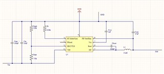
Our customer is using the LMR36506-Q1 and they have this inquiry:

I would like to know what the quiescent current draw is for the LMR36506-Q1 when in standby mode (i.e., VIN less than turn-on voltage) with a turn-on voltage set to 5.5 Volts via the resistor divider at the EN pin.

I see that the datasheet claims 0.5µA current in shutdown and it shows plots of current draw when active, but I cannot find details of current draw during the standby mode that occurs between those two states.

I hope you could help us with this. Thank you.


Regards,

Cedrick

  • Hello

    Please specify the exact conditions for input voltage and EN voltage for this test.

    Also, if you have a schematic you can share that would be helpful.

    Thanks

  • Hello

    I have not hear back from you in one week.

    I will close this post due to inactivity.

    If you need more assistance you can re-open.

    Thanks

  • Hi Frank,

    I apologize for the delay on my response. I've just got back after being sick.

    Kindly see the schematic below.


    Additionally, here's what our customer said: For our particular application, we're particularly concerned about how much input current draw occurs when the input voltage is anywhere below 5 Volts. The datasheet explains the expected current draw in full shutdown (EN line below 0.4 V, equivalent to input voltage of 1.73V in our circuit), but doesn't give details of actual current in standby mode.
    Thank you for your help

    Regards,

    Cedrick

  •  Hello

    Please confirm the load on the device for this testing and the output voltage.

    Also be sure you are using the correct fixed output voltage option.

    The input current will have to be tested in the lab.

    You can test this with a modified EVM.  You will need to replace the device

    with the fixed voltage option and fix the voltage divider.

    If you need TI to take this data, it will be late next week before we can get this work started.

    Thanks

  • I have not seen any activity on this post for more than a week.

    I will close.  You can re-open if you need more help.

    Thanks

  • Hi Frank,

    Thank you for your help in this.

    I've just got a feedback from our customer and here's what they have told us:

    Hello. Sorry for not responding for so long. We did perform this testing in our lab and collected some additional information that satisfies us for now. We find that the quiescent current increases suddenly from <1µA to on the order of 50 µA at some point between 0.4V and 1V on the enable input line. We had to choose a higher turn-on voltage (by selecting appropriate resistors) to ensure that the quiescent current draw stayed low enough through the voltage range we're interested in.

    This works for us for the time being. However, we're relying on undocumented functionality of the IC, so if something in this undocumented operating region changes in the future, it could impact our design.

    I will accept the solution for now but I would like to see this operating region documented more clearly (preferably in the datasheet) with expected quiescent current vs enable pin voltage (assuming that is primarily what determines the quiescent current draw).

    By the way, for this particular work, we were using the fixed 3.3V part and expecting an output load of less than 10 mA when 3.3V is present. However, the region we're interested in is where the output is disabled (Voltage at Enable Pin less than 1.263 Volts).


    Regards,

    Cedrick

  • Hello

    Thank you for this feedback.

    We will consider what can be done in the future to present this type of information.

    Thanks