This thread has been locked.

If you have a related question, please click the "Ask a related question" button in the top right corner. The newly created question will be automatically linked to this question.

CSD18542KTT: Need to verify the schematic for CSD18542KTT.

Part Number: CSD18542KTT
Other Parts Discussed in Thread: UCC27511, CSD18510Q5B, CSD18536KTT, CSD18512Q5B, CSD18563Q5A, CSD19505KTT, CSD19505KCS, UCC27525

Dear Expert,

I can't simulate this circuit in pspice, Is this mosfet circuit is right or not, If wrong kindly help me to built better circuit.

 CSD18542KTT

  • Hello Naveen,

    Thanks for your interest in TI FETs. Your schematic looks OK. Can you please provide more details on the problems you're having with your simulation? For example, are you having convergence issues?

    Best Regards,

    John Wallace

    TI FET Applications

  • Hello John,

    I'm new to the power MOSFETs. I don't know the simulation for this,So I did some study finally I chose this MOSFET and driver.Still I have some doubt in voltage level of IN+ and 12v gate voltage.can you clear my doubt.

  • Naveen,

    John is away on vacation, he is our modeling expert for MOSFET, he will be able to get back to you next week when he returns.

    I apologize for the inconvenience, can you wait until next week?

  • Dear Chris,

    Thanks for your reply. Can you guide me to built better circuit.

  • Naveen,

    I am sorry but no I can not , John is our applications support for MOSFET, can you wait until next week?

  • Dear Chris,

    Thanks! I'll wait.

  • Hi Naveen,

    Thanks again for your interest in TI FETs. To answer your questions:

    1. 12V gate drive will work fine with the CSD18542KTT which has absolute maximum VGS = +/-20V.
    2. For this chopper motor drive application, IN+ should be driven with a PWM signal as shown in the UCC27511 datasheet. Typical input high is 2.2V and input low is 1.2V.

    In addition, the gate resistors may need to be adjusted to get the desired rise and fall times for the FET. 100 ohms may be too large depending on your requirements.

    Lastly, can you share your PSpice simulation with me?

    Thanks,

    John Wallace

    TI FET applications

  • Dear sir,

    I changed the Driver and Mosfet due to due to component availability.Here below I attached the schematic please verify.I'm going to use 48v 40A.

  • Hi Naveen,

    Your schematic looks good. However, the power dissipation at 40A will exceed the capability of this device which is about 2.5W max. The conduction loss at TJ = 25°C is 40A x 40A x 14.5mΩ = 23.2W. Please see this technical article for more information on power dissipation capability of TI FETs. You will need to select a FET with lower on resistance for this application. Please take a look at the CSD18536KTT, TI's lowest on resistance FET in D2PAK. You might also consider the CSD18510Q5B or the CSD18512Q5B in 5x6mm SON package.

    Best Regards,

    John

  • Dear sir,

    Can I use this Mosfet CSD18563Q5A.

  • Hello Naveen,

    The maximum on resistance of the CSD18563Q5A is 6.8mΩ at VGS = 10V & TJ = 25°C. The conduction loss at 40A is 10.88W not including the positive tempco of on resistance (see Figure 8 in the datasheet). The 5x6mm SON package can dissipate a maximum of about 3W with a good layout on a multilayer PCB. You can parallel FETs to reduce the conduction loss and spread the power dissipation over multiple devices with a greater surface area. With this approach, the conduction loss is reduced by the number of FETs in parallel and dissipation in each device is the total divided by the number of parallel FETs. For example, if you parallel two FETs the total conduction loss is reduced by 50% and each device dissipates 50% of the total conduction loss. At 40A, the total conduction loss would be 5.44W and in each CSD18546Q5A it would be 2.72W.  Gate drive and switching losses would increase but motor drives typically switch at lower frequency (around 20kHz) and conduction loss is dominant.

    Thanks,

    John

  • Dear Sir,

    I dont have that much experience with parallel mosfet So I choosed CSD19505KTT.This Mosfet have very low Rds 2.6mΩ at VGS = 10V.

  • Hi Naveen,

    The CSD19505KTT is a good FET for motor drive applications. The conduction loss at 40A is 40A x 40A x 3.1mΩ (max) = 4.96W and will exceed the capability of the package.Can you share more details about your application? Is 40A the continuous rms current or is this peak?

    Thanks,

    John

  • Dear sir,

    This is the Peak current only and I'm going to use CSD19505KCS Which is TO-220 Package.

  • Dear Sir,

    Can I use this Mosfet?

  • Naveen,

    Thanks again for your interest in TI FETs. Yes, this MOSFET can be used in your application. The TO220 package can be attached to a heatsink to help remove dissipated power from the device.

    Best Regards,

    John Wallace

    TI FET Applications

  • Dear Sir,

    Can I use UCC27525D with 3.3V GPIO MCU for this Mosfet.

  • Naveen,

    Thanks for reaching out and for your interest in TI parts!  My name is Aaron Grgurich and I am the applications engineer for the UCC2752X family of gate drivers.

    -------

    Yes, if the input pin(s) of the UCC27525 are driven by a signal from 0V to 3.3V, that will work.  This is outlined in Section 7.5 of the datasheet.

    -------

    I hope this answers your question!  If so, please press the green button; otherwise feel free to follow up!

    Thanks,

    Aaron Grgurich

  • Hello sir,

    Can I use this driver with P-CH Mosfet?

  • Hi Naveen,

    Yes, you can drive a P-Channel MOSFET.  To protect your power-FETs, consider having a 10 kOhm or 20 kOhm resistor from the gate to source to ensure the FET stays off during power up (a pull-up resistor on the gate).

    Thanks,

    Aaron Grgurich

  • Hello Sir,

    Could you please check the below Circuit and give the update.

  • Naveen,

    Sorry, I forgot to look at the schematic again... with a bus voltage of +48V, you CANNOT use this gate driver with a PMOS here.  I would suggest using a NMOS MOSFET.  NMOS MOSFETS switch faster and have less R_DS On than PMOS as well (as a general rule of thumb).

    I still have design suggestions for if you switch back to an NMOS design.

    -------

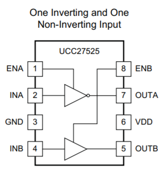
    Please note that the UCC27525's INA is inverting and that INB is non-inverting.  Please make sure this is what you want (this seems good to me)

    Here are my comments on the design:

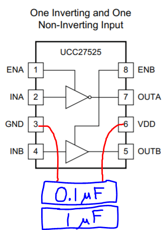
    1)  Regarding the V_DD capacitor bypassing, please reference Section 8.3.1 of the datasheet.  You should put a 100nF (0.1uF) capacitor as close as possible to the IC and a 1uF in parallel right next to the 100nF.  Please see the image below for how to layout the capacitors.


    2)  Depending on how noisy the system is, you may need input signal filtering.  At a minimum, you should put place holders for a low-pass filter into the input  (The place holders would be a 0 Ohm short resistor, and do not populate the capacitor).  If you end up populating the low-pass filter, do not put a resistor any larger than 100 Ohm and a capacitor any larger that 200 pF.)

    3)  It may not be a bad idea to ground INB, but it is not needed (since it is not being used).

    4)  R4 should be from the gate to source of the power MOSFET (This was correct on your original schematic)

    -------

    Sorry again for missing the schematic on your PMOS question, but I hope the above helps you.

    -------

    I hope this answers your question.  If so, please press the green button; otherwise feel free to follow up.

    Thanks!

    Aaron Grgurich