This thread has been locked.

If you have a related question, please click the "Ask a related question" button in the top right corner. The newly created question will be automatically linked to this question.

LM5175: Weird switching behaviour/ high Iq at some input voltages

Part Number: LM5175

I'm trying to design a buck boost regulator with the LM5175. I need to convert 23-33.6V (8s lithium cells) to stable 24V @ 5A.
I have created schematic and layout, based on LM5175EVM-HD and the excel calculator tool.

Enable resistors are 0 ohm, because I was planning on fitting some resistors afterwards to do UVLO testing. Now EN is tied to VIN with 0 ohm resistor.
Mode resistors are also placed like this to do testing, 100K to gnd is fitted now, which should result in CCM operation with hiccup enabled.
RC snubber values have just been copied from a reference design and must be calculated afterwards (if necessary). They are fitted now as per the schematic.

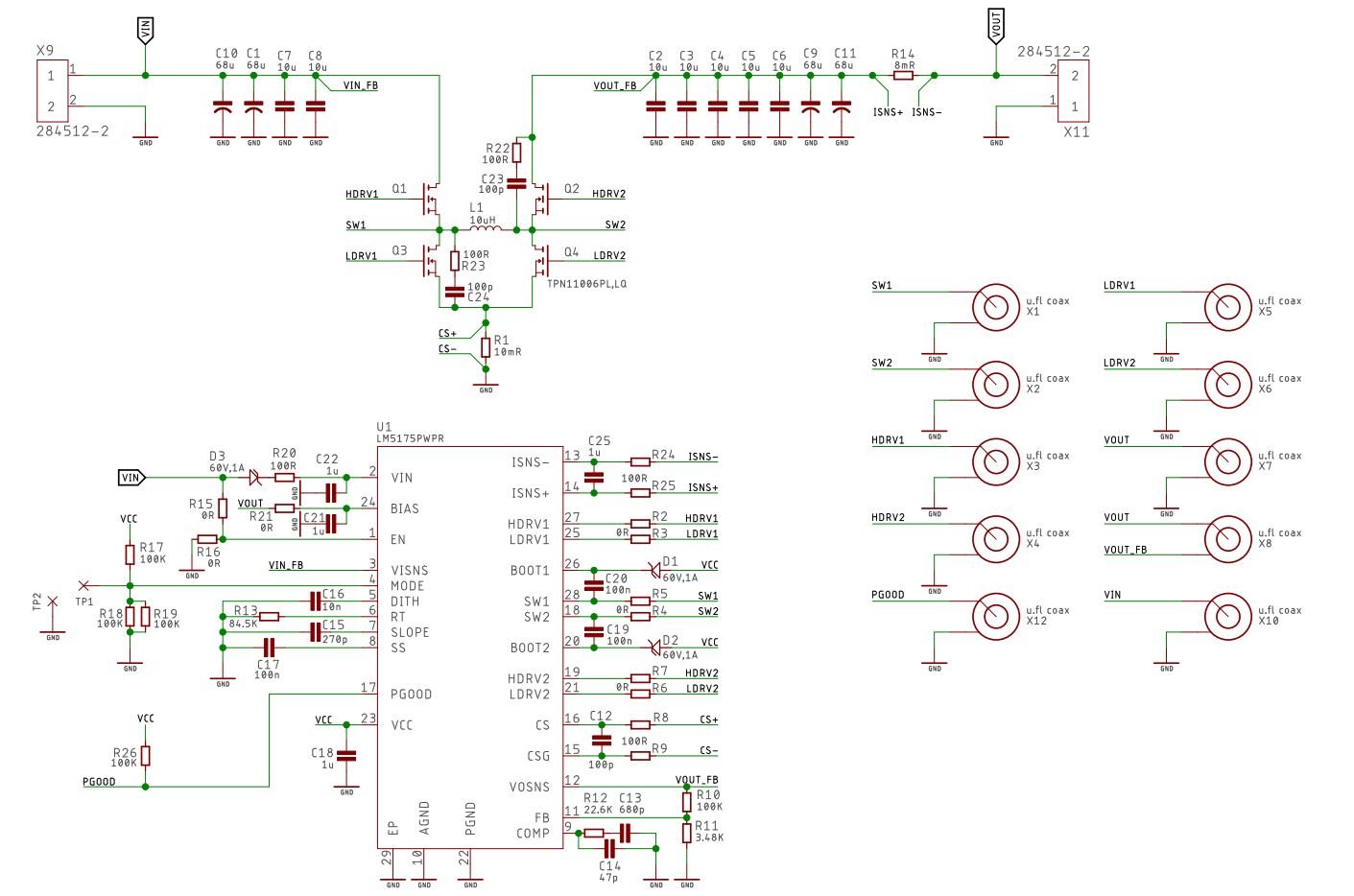
Here is the schematic:

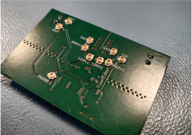
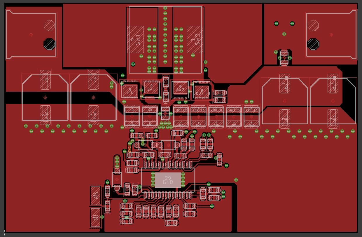
Here is the board layout. Only top copper is shown since the rest is mostly GND plane. Bottom layer (4 layer board) is used for gate signals and current measurement signals

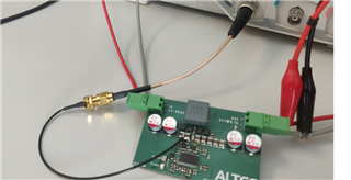
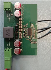
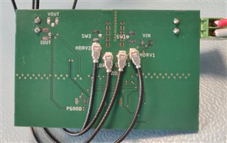
Here is the test setup:

The circuit is outputting 24V, so that is working. At some input voltages the circuit is stable and I can supply 5A load with 96.5% efficiency. The inductor and mosfets are not the lowest DCR/Rds types so this is fine. Iq is a bit high with 35mA. There are some problems though. I feel like the switching can become unstable depending on input voltage and load current.

What I have observed:

-boost mosfets start switching when well into buck mode (28Vin, 24Vout)
-buck fets start switching when well into boost mode (20V in, 24Vout)
-in some switching cycles the gate drive signals get horrible ringing which is also visible on the SW1/SW2 and Vin/Vout node
-when the above stated condition occurs the Iq of the entire circuit (no load) becomes horrible (>70-150mA).
-with some input voltages the efficiency also dips drastically, making the circuit to dissipate large amounts of heat.

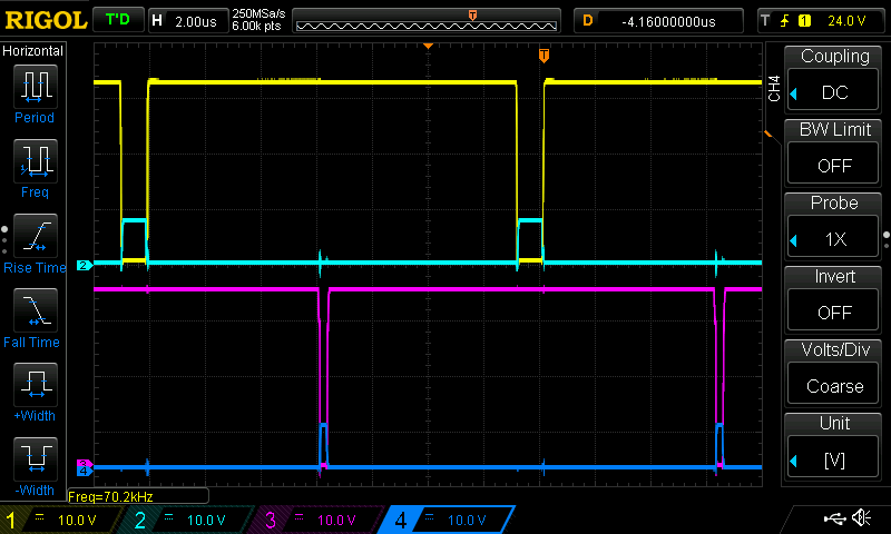
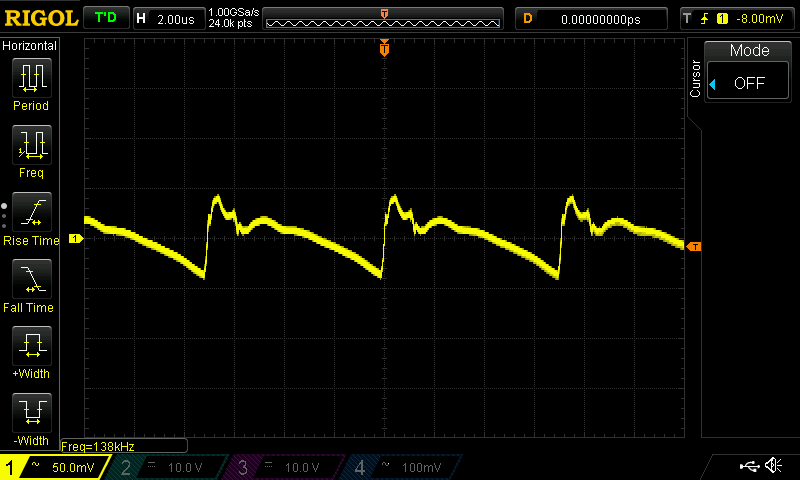
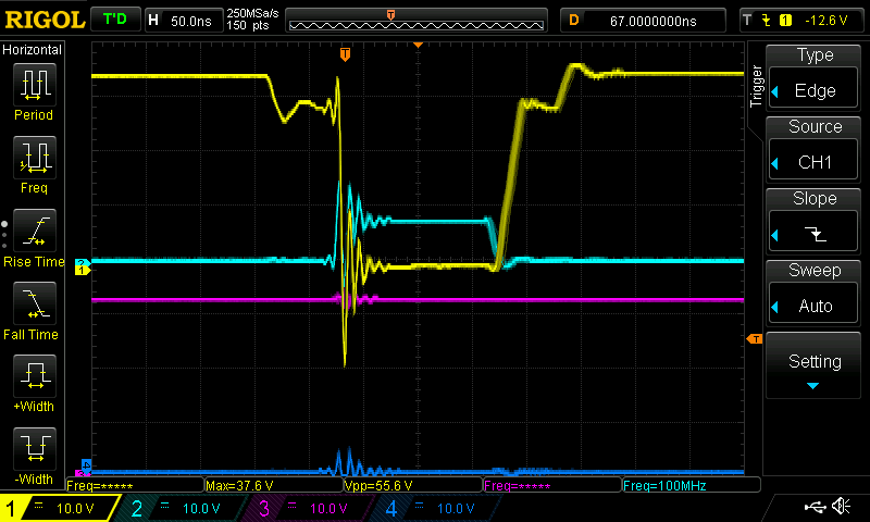
These are the HDRV1 (1), LDRV1 (2), HDRV2 (3) and LDRV2 (4) signals:
at 32Vin the signal is looking pretty nice, and the boost side driver has no activity as expected in buck mode. Iq is 35mA.

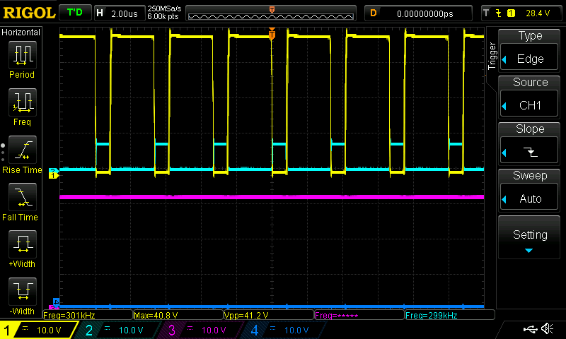
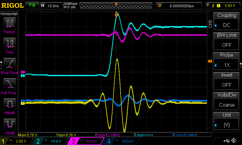
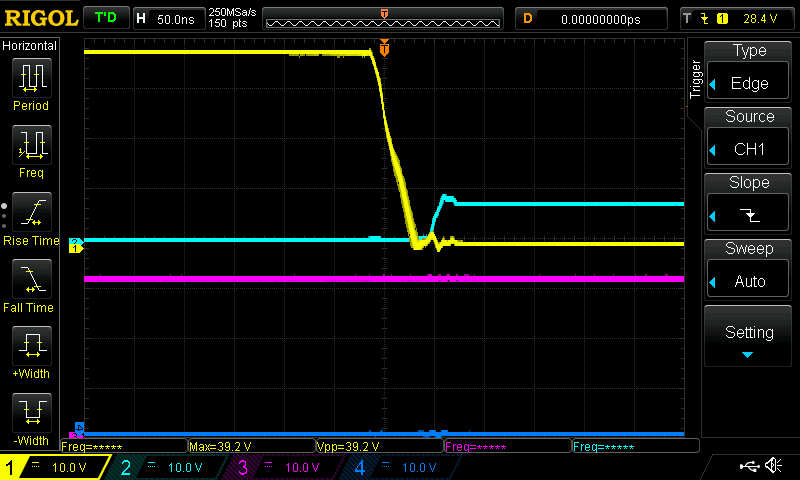
zoomed in HDRV1 and LDRV1 shows nice transition, also good dead time so I assume the fets are not conducting at the same time.

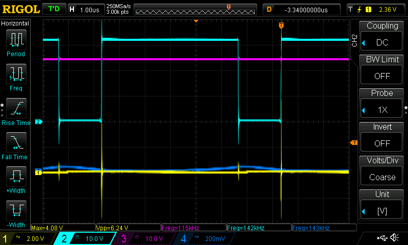
But when the input is reduced to 29V, the driver signals starts looking pretty bad, and the Iq increases to 100mA. Both IC and inductor start heating up.
Also HDRV2 and LDRV2 start switching for some reason:

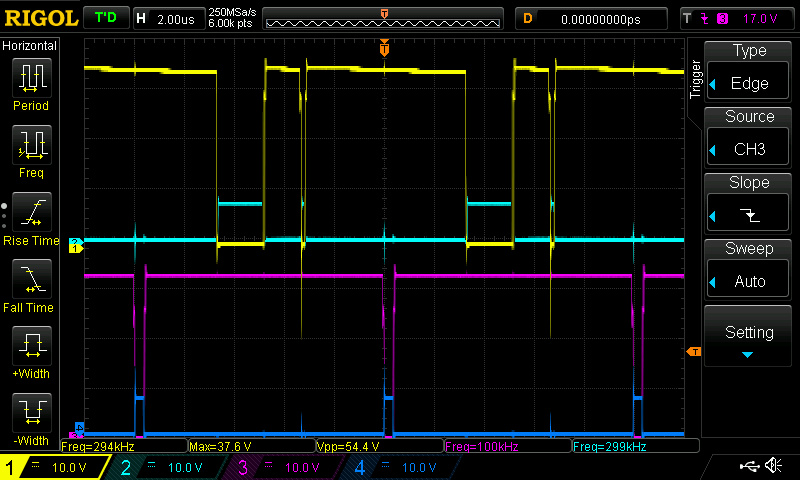
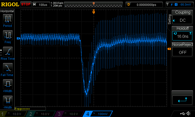
Now zoomed in HDRV1 and LDRV1 shows pretty bad ringing, and to me it seems like both fets are conducting for very short time, like HDRV1 is held by something for a few 10's of ns.
The bad ringing signal also can be seen in HDRV2 and LDR2

I'm no expert with these types of regulators. I can only suspect some kind of instability. The excel calculator shows the following chart with my component values:

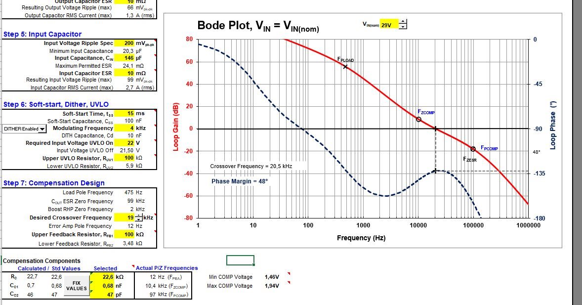
comp voltage is measured around 1.6V, so that seems to be alright.

The gate driver signals above are captured with no load at the output. When the instability occurs with a loaded output, the efficiency drops drastically causing the entire thing to heat up quickly.
On a final note, the ringing of the gate signals (4th scope image) is also visible as (or caused by?) quite substantial Vin / Vout ringing (few volts). It won't hurt our application but I doubt that's good for EMI.

Any kind of help or insight as to what might be causing these instabilities would be hugely helpful. Would changing gate resistors and compensation components be a good place to start?

polymer input/output caps: https://nl.mouser.com/datasheet/2/212/1/KEM_A4088_A768-1864506.pdf
ceramic input/output caps: https://nl.mouser.com/datasheet/2/396/TaiyoYuden_UMR325AC7106MM-P_SS-1888209.pdf
I
nductor: https://www.bourns.com/docs/Product-Datasheets/SRP1265A.pdf (10uH)
FET's: https://toshiba.semicon-storage.com/info/docget.jsp?did=54662&prodName=TPN11006PL

  • Hello, 

    Thank you for designing with the LM5175. Sorry for the delay because of extended PTO around the Labor Day holiday. We will study this case and get back to you by COB Thursday this week.

    Thanks,

    Youhao Xi, Applications Engineering

  • Dear Youhao,
     
    I'm very curious as to what might be the issue in my design. If you need any further information please let me know.
    I have attached a PDF of the schematic, it might be more easy to read compared to that screenshot in my original post.
    Thanks for looking into the matter!

    buck-boost proto.pdf

    Cheers,
    Thijs
     

  • Hi Thijs,

    Again sorry for the delay.  I reviewed your layout and schematic and below are my comments which you can try to see if there any improvement.

    Regarding the switching ringing, could you make R2=R3=R6=R7=1 Ohm.

    Regarding the operation at 29V, the circuit seems entering the buck-boost transition mode. Could you change the following components and see if the circuit can be more stabilized at 29Vin?

    • C15=100pF
    • R12=10k
    • C13=15nF
    • C14=470pF

    Thanks,

    Youhao 

  • Dear Youhao,

    This time I'll apologize for the delay. Sadly, our electronic load died during my testing (I hope not because of this psu board) so it took a few days to test the circuit under load. But I did get around to make the changes you suggested. I did not have the exact values on hand, but did manage to make some progress. I have used these values:

    • C15=100pF
    • R12=10k
    • C13=10nF
    • C14=680pF
    • R2=R3=R6=R7=5 Ohm (10//10).

    What I noticed is that the LM5175 is entering buck-boost transition mode as soon as the off-time of the HDRV1 and LDRV1 goes below few 100 ns.
    When the switching frequency was lowered from 300KHz to 150KHz, this would occur at around 27V instead of 29V. I did choose the inductor value quite high in contrast to existing reference designs, as to keep the ripple current at 33.6Vin (max Vin for this design) around 1/3 of average current. I might look into this some more. I'm planning to also add USB-C charging capability after seeing the PMP20774 reference design using this very same IC. Outputting 5V from 33V might be easier with the higher value inductor.

    The circuit is very stable in buck-boost transition mode. with 24V->24V conversion, the circuit operates at 97.7% efficiency with a 5A load and barely gets hot. Those short transients during the buck-boost transition are gone, and all seems to be working well. 

    The gate resistors are now 5R. It did help a lot with the ringing. Power dissipation in the fets seems not to be affected at all. The following signals were captured with the circuit supplying 1A load current at 25Vin: HDRV1 (1) LDRV1 (2) HDRV2 (3) LDRV2 (4)

    gate switching signals 1A load

    Even with the new compensation components the response for load transients is quite good. This shows a 0 to 4A load transient on Vout:

    Just one final issue I ran into: the VIN node is showing very high voltage transients. It seems this occurs when SW1 is being pulled high (during buck-mode operation). The highest transients on the ouput are about 500mVpp during switching. For the input this is almost 10Vpp, even tough the ceramic and bulk capacitance on input and ouput is very similar. I added two 10uF 50V and one 100nF 50V ceramic capacitor, but this didn't seem to do anything.
    Screenshots below show Vin (1) at ceramic input capacitor, SW1 (2), SW2 (3) and Vout (4) after current shunt:

    Vin ripple

    zoomed in on rising edge of SW1:

    Vin ripple zoomed in

    That 10Vpp ripple seems reason to worry. Do you have any idea as to what could cause this behavior? Could it have anything to do with the RC snubbers? I have simply copied the values of reference designs, so it might be doing more wrong than good here.

    Thanks a lot for these tips up to now, it has been tremendously helpful. 

    -Thijs

  • Hi Thijs,

    Thank you for the updates, and I am glad to hear the improvements.  Regarding the Vin ringing, the measurement may be false owing to the long ground lead of the regular probe.  Could you use the short ground lead as shown in the attached picture, and place it across your capacitors? 

    Regarding the 500mV undershoot in the output voltage, it can usually be reduce by (1) adding more output capacitors, and/or (2) to increase the loop crossover frequency.  

    Thanks,

    Youhao

  • Dear Youhao,

    The measurements were taken via u.fl coax connectors on the bottom side of the PCB. This is then adapted to SMA, and then with another cable to BNC. the total length of the coax is about 30cm. Turns out this is still not good enough. For this measurement I have just snipped off the u.fl connector and soldered the coax directly to the input cap:


    Ripple seems normal to me now. Managed to lower it a bit after adding 100nF an 10uF capacitor:

    As for the over/undershoot during load transients, what we have now is more than fine for our application. Since it seems to be very stable now, I won't touch it further. 

    Thanks for the support!

    -Thijs