Other Parts Discussed in Thread: DAC39J84EVM,
Hi,
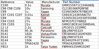
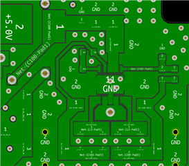
I was using the TPS62420DRCR to generate 2.5V and 0.9V DC with a 5.0V input. However, I always measured around 0.3V output voltage on both SW1 and SW2 outputs. The DEF_1 and ADJ2 voltages were measured to be 0.07V and 0.2V respectively, which made me think that the external resistor network was working (the voltage ratio matched the resistor ratio: 0.07/150*(150+475)=0.3V, 0.2/182*(182+95.3)=0.3V). But the DEF_1 and ADJ2 voltages were still much lower than the TPS62420DRCR reference voltage, which should be 0.6V. Attached are the schematic, BOM, and layout for my PCB. I followed the TPS62420DRCR design in the DAC39J84EVM schematic, except that I used an available part to replace the obsolete part for C95 and C105. Does anyone have any thoughts of why the output voltage is so low and the reference is not 0.6V?

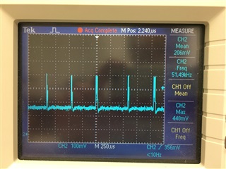
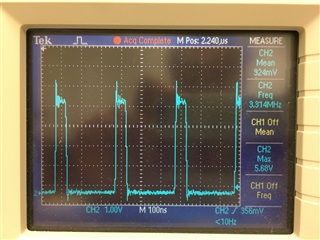
To debug this issue, I tried the following test on the SW1 line. Removed L3, C103, C106, and C107. Applied and adjusted the DC voltage with a voltage source on U13 pin 4, then measured the response on pin 5 and pin 6 of U13 with an oscilloscope. Only when the 3.5V DC voltage was applied on pin 4, I could see the PWM transition and the feedback loop started to work. At this time, pin 5 and pin 6 was measured to be 0.6V and 3.5V.
Thanks and best,
Yilun