Hi Sir,
My customer has a issue about the MCLK output 40MHz or did not any output. They have some questions for power-up timing sequence as below.
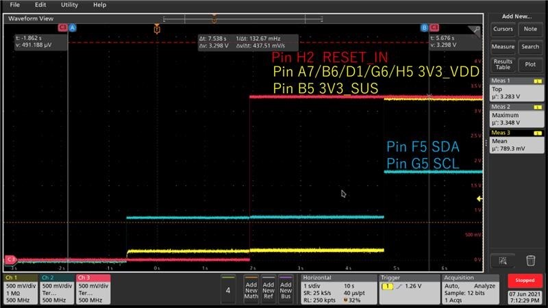
1. Only 3V3_SUS and 3V3_VDD are specified in the datasheet 8.3.1 ) of TPS68470, could you tell us the detailed power sequence requirements? need the timing sequence between the I2C pull-up and the Reset pin?
2. When the I/O power is done before the 3V3_SUS and 3V3_VDD, what kind of malfunction can occur with the power sequence on the below?
SDA/SCL => RESET_IN => 3V3_SUS/3V3_VDD