This thread has been locked.

If you have a related question, please click the "Ask a related question" button in the top right corner. The newly created question will be automatically linked to this question.

TPS40077: layout review

Part Number: TPS40077

Dear team

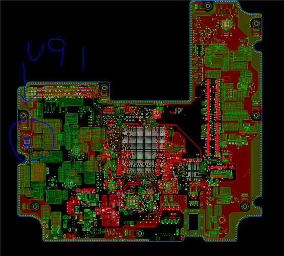
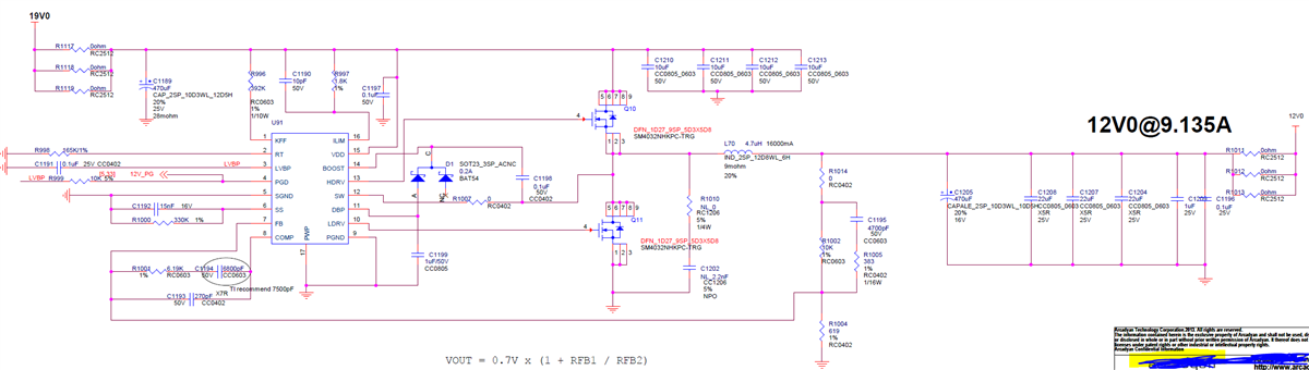
There is a good news that we design in TPS40077(U91) in customer's new project.

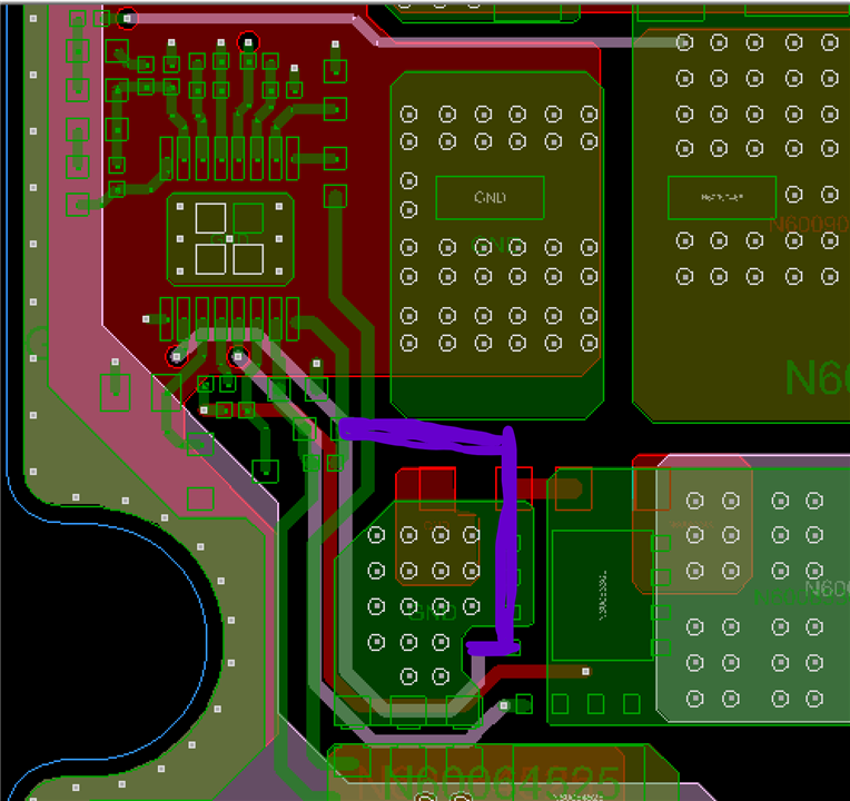
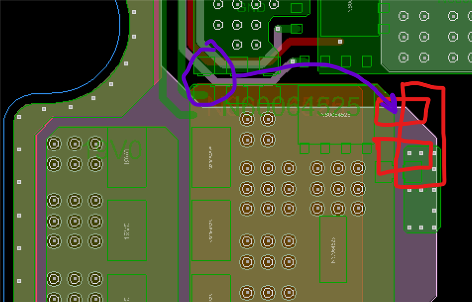
Could you help to review the Layout?

3618.BS72RS1400A-ZZ_20210914.brd

Many thanks

Denny

  • Hi Denny,

    Our US team will review it and reply you soon.

  • Denny,

    It will take a couple of days to review the layout.

    Does the BRD file contain only the U91 layout?  If not, can you provide a screen shot showing where U91 is located in the larger board file?

  • Hi Peter

    Sorry for late reply.

    The screen shot of U91.

    Many thanks

    Denny

  • Thank you Denny.

    I will get to this tomorrow.

  • Denny,

    The layout is pretty good, but there are a few places it could be improved.

    The gate drive loops (LDRV to Gate, Gate to source, Source to PGND, HDRV to Gate, Gate to Source, Source to SW) carry high dynamic currents.  They should have 2 vias when changing levels.  I would also recommend they route LDRV under the source pins and back to the LDRV via.

    I would also recommend routing the SW net directly under the HDRV trace.  In addition, I would recommend widening all of these traces to 20 or 30 mils wide.

    I would recommend also increasing the PGND connection to using at least 2 vias, or even better, connect directly to the thermal pad.

    I would recommend increasing the number of vias used to connect the DBP capacitor to GND.

    I would also recommend moving the VIN capacitors on the right side of the high-side FET up closer to the FET as well as moving one of the three on the left to the right side to be closer to the FET and provide a separate loop from the left side.

    Otherwise, things look good.

  • Hi Peter

    I appreciate your great support.

    But the customer would like to double confirm  some suggest. Could you help to recommend?

    1. The gate drive loops (LDRV to Gate, Gate to source, Source to PGND, HDRV to Gate, Gate to Source, Source to SW) carry high dynamic currents.  They should have 2 vias when changing levels. 

    => The 2 vias means : top layer need add one via as shown below.

    I would also recommend they route LDRV under the source pins and back to the LDRV via.

    => The trace of LDRV route under source pins, Does have any concern?

    Many thanks

    Denny

  • => The 2 vias means : top layer need add one via as shown below.

    Yes, two vias each time the signal changes layers.

    => The trace of LDRV route under source pins, Does have any concern?

    Not a major concern, but routing the LDRV with less trace and lower inductance under the Source pins will help reduce low-side GATE rise during the dV/dt rise of the switching node.