This thread has been locked.

If you have a related question, please click the "Ask a related question" button in the top right corner. The newly created question will be automatically linked to this question.

TPS56628: inquire about PG pin

Part Number: TPS56628
Other Parts Discussed in Thread: TLV7041,

Hi TI experts,

Customer did using TLV7041 + TPS56628. but customer plan to change TLV7041(open drain comparator) to TS2111(normal OPAMP) because of TLV7041 L/T issue.

TPS56628 PG pin and opamp output are connected. TLV7041 is open-drain, so it doesn't matter, but TS2111 is an opamp output.

We are concerned about the internal FET damage of the TPS56628 PG pin.

When 1.5V power is output, OPAMP is output high. However, the PG of TPS56628 hold low.

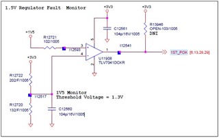
When the TPS56628 power is output normally, the PG becomes high and the final 1ST_POK net is output as high.

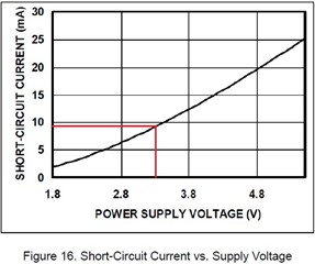
Output current of TP2111 is 20mA.

But PG sink current of TPS56628 is 4mA.

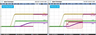
TLV7041 vs TP2111 wave form

If the customer uses TS2111, is there a possibility that the PG pin of the TPS56628 will be damaged?

Please check it.

Thank you.

  • Hi Kim,

    I will check it and feedback you by early next week.

  • Hi Kim,

    We discussed internally, there's possibility TPS56628 PG-pin may damage in this application. TS2111 20mA output capability is too strong for TPS56628, may generate large power and damage PG-pin.

    Please choose another comparator/OPAMP. You can consult e2e Amplifiers forum, find an alternative to replace TLV7041.

  • Hi Miranda,

    Customers use VCC power of TS2111 with 3.3V. Therefore, the opamp output current is expected to be 9-10 mA.

    And the time for PG pin to keep the opamp output low is 3.7 ms.

    Still, is there a possibility that the PG pin will be damaged?

    What is the maximum allowable current of the PG pin?

    Thank you.

  • Hi Downey,

    Thanks for the explanation. 

    We would normally recommend to limit the allowable current smaller than PG sink current ability. When source current is higher than PG sink ability, internal Mos could work in saturation region. The damage of Mos is not determined by one factor. When large Vgs, Vds and Id occur same time, the risk for Mosfet damage is high.

    You mentioned about the PG pull-low time and estimated opamp current. That's the behavior of normal startup. I would have some concern on some possible corner case in customer's application which could trigger large Vgs, Vds and Id of internal Mos at same time. And we cannot guarantee the long term reliability and performance when device is not used according to our recommended spec.

    Thanks,

    Andrew