This thread has been locked.

If you have a related question, please click the "Ask a related question" button in the top right corner. The newly created question will be automatically linked to this question.

UC2827-1: Push/Pull Jitters as Wattage is increased.

Part Number: UC2827-1


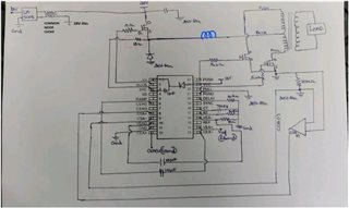
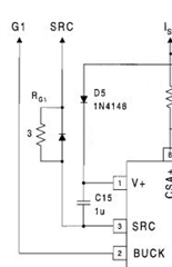
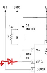
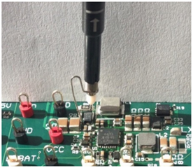
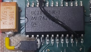
The SCR was 5.6 Ohm  highlighted in red box.


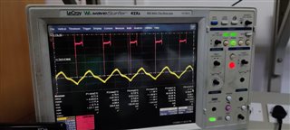
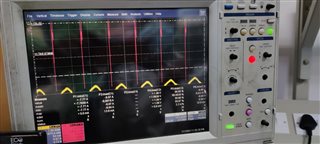
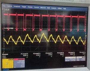
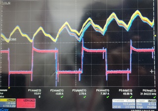
The functionality of  our topology was working fine with 90W . The below image is give for the for Vgs of Push/Pull Mosfet and the Buck Current.
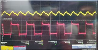

Where the
Pink  -  Vgs of the Push section .
Yellow  -  Buck Current.

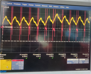
As we increased the wattage above 90W, We observed a jitter in Push/pull Vgs.

The Push/Pull Vgs was abnormal with jitters of 1us-2us reciprocating a change in the buck current as shown below
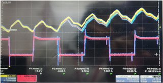
where the
Pink - Vgs of the Push section
Yellow  -  Buck Current

The SRC resistor a was increased from 5.6 Ohm to 12 Ohm. There were no such jitters from 90w to  115w
As the Wattage of the converter was increased to 120W. The push/Pull Vgs were jittering as shown above waveform .

We cannot increase the SRC resistor above 12 Ohm

We are stuck to proceed further. Guide me to solve this problem.

  •  Part Number: UC2827-1

    Hi  everyone!

    We are using UC2827 - 1 (Current fed ) in our application. A cascaded Buck with Push Pull converter. The Sch below is just for understanding the topology as we are not authorized to share the complete circuit schematics.

  • Hello Bob,

    This is difficult to understand without a schematic.  For example, where is the SCR (or SRC) resistor?

    What are the input voltage, output voltage, and switching frequency?

    When you see the jitter, what does the current from the buck look like on a longer time base?  Is the buck becoming unstable?

    Please send the schematic to my email address and I will respond ASAP; e-reicher@ti.com

  • Dear
    The Input voltage is 28V
    Buck Voltage is 24V @ 85% duty
    Output Voltage at Push/pull is Vtop = 50V and Vmax = 130V
    Rt =20K, Ct = 750pF,
    Switching Frequency is 51KHz
    The buck current is unstable in long time span as sown in the below images

  • Hello Bob,

    I don't see a buck inductor in your schematic.

    Could you review the following Design Note.  Figures 5 and 12 and the Design section should help you quite a bit.

    https://www.ti.com/seclit/ml/slup117/slup117.pdf

    Regards,

    Eric

  • Dear Eric,

    Sorry the Inductor was not drawn. Kindly the updated Schematic with the Inductor.

    We have carried as per recommended the design Note.

  • Hello Bob,

    In the Application Note they added a 3 ohm SRC resistor, and used a diode in parallel with it (see below).  This is a current limit resistor because the SRC pin is forced negative when the free-wheeling buck diode conducts.  I would like to try a few things for your circuit.  First, make sure the free-wheeling buck diode is a Schottky type and is large enough to maintain the negative voltage as close to 0V as possible (say -0.2V to -0.4V) at full load.  Second, try adding a diode in parallel with the SRC resistor as they did in the following figure (anode at the SRC pin).  Lastly, check the PCB layout and make sure the GND, PGND, and anode of the free-wheeling diode are all directly connected (no vias) with as short a loop as possible (i.e. no inductance).

    I thought of one more thing to try.  If we want to limit the negative voltage at the SRC pin we can add a Schottky diode from GND to SRC as shown below.  This should be a 1A or 2A rated diode.  Add this diode very close to the SRC pin.


  • The free-wheeling diode is a Schottky diode as recommended.

    The SRC pin was probed before changes, The observed shoot was -3.5V

    As first recommended, while a diode was placed parallel to SRC resistor the Buck current oscillation occurred even earlier to existing configuration. A Negative shoot of 5V was observed while placing Diode parallel to SRC resistor.

    Before Oscillation

    While oscillation the negative shoot reaches to 6.6V. Hence we removed the diode and tried further

    Secondly, The PGND,GND and Anode of the Free-wheeling diode was also placed the shortest possible. – No improvement.

    As recommended, Placing Schottky diode from GND to SRC as shown to limit the negative voltage reduced the shoot 2.5V leading slight increased power of 2 W at output. The wave form at SRC Pin with Buck Current is as follow.

    Pink – Vsrc with respect to PGND

    Yellow – Buck current

    Kindly suggestion to proceed further to increase the wattage.

  • Hello Bob,

    The high-frequency spikes to -2.5V are often a result of the long ground lead on the 'scope probe.  If you use a tip-and-barrel measurement at the SRC pin you will see the real voltage at the SRC pin.  Tip-and-barrel measurement technique is shown in the following picture.

    As far as increasing the wattage further:

    I see the duty cycle increasing when the buck current rises.  You need to resolve the instability.  Do you have the ability to examine the bode plot for gain and phase margins at 90W or 115W?  Is the inductor rated to handle the current at 120W?  Do you have enough input and output capacitance?  Without a detailed schematic I don't know what else to recommend.

  • Dear Eric,

    Yeah, the inductor is rated to 24A, the actual RMS current is 7A and enough input and output capacitance are provided.

    Yeah we can examine bode plot.

    As the duty cycle increases as the current rises,but is there  a possibility for the Push pull frequency jitter due to instability in control loop compensation

  • Hi Bob,

    The frequency of the current oscillation you showed was about 2.5 kHz.  This frequency makes me think the issue is with the current loop compensation.  I don't have a clear understanding of how you are using the part because I don't have a full schematic of the regulator.  Assuming it's peak current mode control, I would try a Type-II compensation instead of the simple Type I (only a 10uF feedback capacitor), making sure your have an RC filter to the current sense input, and adding slope compensation if you don't have it already.

    Regards,

    Eric

  • Dear Eric,

    Thanks for your suggestions.

    As per data-sheet,  the push-pull Vgs should be generated independently at close to 50% duty cycles without giving any control signals such as voltage /current control.

    The above functionality of Push pull Vgs generation was already been verified and found ok without giving any control signals..

    But in this case,Frequency shift/jitter observed in Vgs of  push pull pin -IC, when increasing output power.Since we are using current fed PWM controller, there is no output capacitor at buck output -only buck inductor was used.

    So we believe that, this Frequency shift in PUSH PULL- Vgs could be thee reason for the oscillations of buck current.-refer attachment

    Pink- Vgs of Push/Pull

    Yellow-  Buck current


    It would be better, if we found the reason for oscillation in Push-Pull Vgs  to resolve this issue.

    Temporarily we have used 10uF as feed back capacitor for voltage/current error amplifier to neglect control loop related problem(ie., since we are using 10uF capacitor, operating cross over frequency of this system should be in the range of Hz). Once after verification of other functionalities is completed, we will look into Loop compensation.-FYI

  • I've seen negative voltages disrupt an IC - the reference voltage and frequency begin to shift when parasitic PN junctions begin to turn on.  In your case the SRC resistor and the Schottky diode at the SRC pin of the IC definitely helped.  So I would investigate if there is any way to further reduce the negative voltage(s).

  • Dear Eric,

    Thanks for your suggestion.

    As recommended the Schottky diode at the SRC Pin, helped to limit the negative voltage ( below  -0.450V ).

     In our case, we used jumper cable of 30 AWG  to short  PGND and GND from IC pin 11 to pin 21.(Length of 35mm).

    Will increasing the short path with higher AWG (for example 18AWG or Litz cable ) would improve the grounding?

    In our case, the Negative voltage is reduced as recommended yet the issue remains.

  • Hi Bob,

    35mm is longer than I would prefer and 30AWG is relatively thin.  Is this circuit built on a PCB or wired-up on a proto-board?

    Regards,

    Eric

  • Dear Eric,

    thanks for your responses,

    its wired on a proto-type. 

    regards,

    Robert

  • Dear Eric,


    The frequency jitter did not occur with same wattage as we reduced operating frequency from 53KHz to 44KHz.

    Why is the jitter occuring at higher frequency ?

    But we also observed an another deviation in UC2827DW's oscillator frequency selection using RT and CT

    our configutarion in UC2827DW-1 was 750pF and 20.55K Ohm provides the calculated frequency is 50 KHz, where as the measured frequency is 53KHz.

    Similarly we Also check with UC2827DW-2, where the RT and CT were 19.4K Ohm and 680pF provides the calculated frequency is 58 KHz. Instead the measure frequency was 66KHz


    The Capacitors were measured in house LCR meters also and verfied to be same.

    Why there is a deviation in the frequecny from expected to actual?


    Regards,
    Robert Brolin Anthony S

  • Hi Bob,

    We always recommend some RC filtering on the current sense signal.  Blanking voltage spikes/noise when the FET turns on is critical to having jitter-free regulation.  At lower frequency the "same" noise/spike is a smaller percentage of the on-time so the jitter is often reduced.

    As for the frequency accuracy, the data sheet shows -10%/+13% for 220 kHz with RT=10k and CT=340pF.  Tolerances at other frequencies are not guaranteed to be this low.  In most controllers the frequency tolerance can be as high as +/-20% due to process/manufacturing deviations.

    Eric