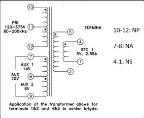
Hello,
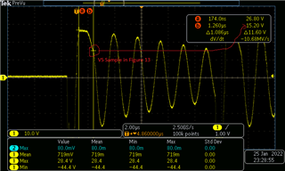
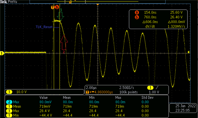
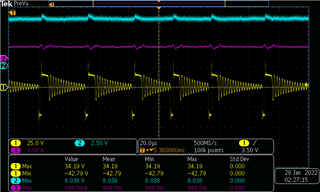
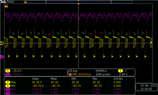
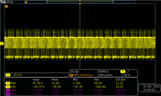
See the figure bellow.
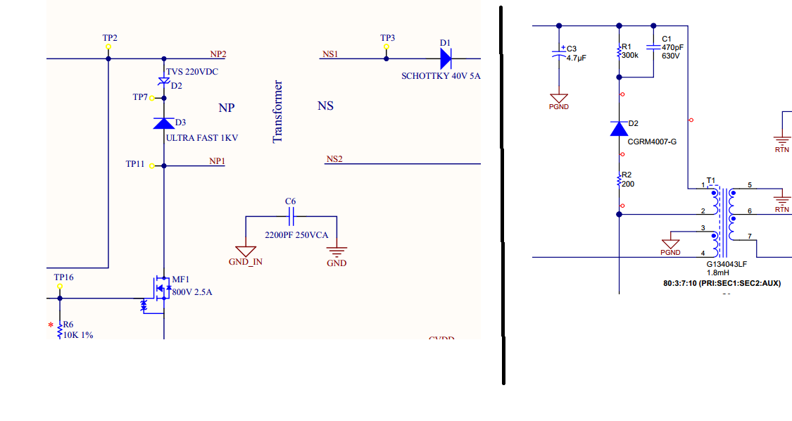
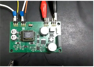
On the left we have my circuit, on the right a circuit found on the texas website.
Question: Some designers do not consider the TVS diode (D2), see the figure on the left.
Could you please tell me why the designers don't consider this TVS diode?