This thread has been locked.

If you have a related question, please click the "Ask a related question" button in the top right corner. The newly created question will be automatically linked to this question.

TPS65185: VDDH fails to start

Part Number: TPS65185

Hi,

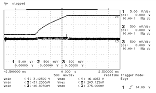
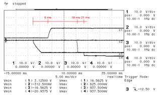
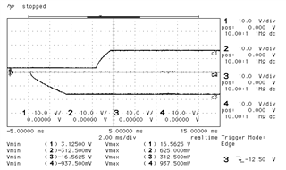
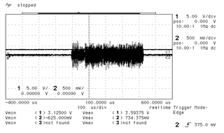
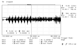
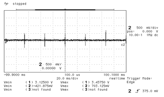
I'm trying to use a TPS65185 to provide power to an E Ink display.  I've designed a board and assembled it, and while 5 out of the 6 voltage rails come up correctly, VDDH seems to fail to start. The PG register indicates that VDDH is not working (but the other 5 are). Probing VDDH with an oscilloscope, I see a "ringing" pattern centered around 0 volts:

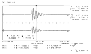
Channel 1 (top) is VDDH, channel 2 (bottom) is VDDH_DRV. (note the location of the ground marker for each channel, on the left. Also note vmin and vmax for each channel, at the bottom)

This pattern repeats continuously until I shutdown the power rails by turning off the PWRUP pin. Is there a reason why this might be happening? I initially thought it could be that I was missing some capacitors, but I checked and my schematic seems to match the EVM and recommendations in the datasheet.

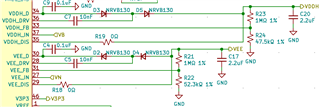
I assume there's probably an issue with my layout? Looking at it now, I can make some guesses as to what might be wrong:

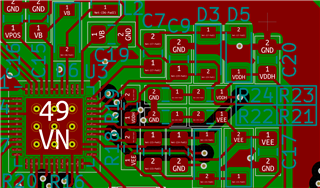
  • all the traces are the same width (0.2 mm = 7.9 mils) - some of the power traces should probably be wider?
  • the board only has two layers, so the ground plane cannot fill everywhere and there's no +3V3 plane
  • the capacitors and diodes for VDDH might be too far from the TPS65185?

However, I'm not really sure how those issues would cause this behavior. Any feedback and/or troubleshooting suggestions would be greatly appreciated!

The relevant parts of the schematic and layout are attached below (sorry they're a bit messy). I can also upload the rest of the schematic and/or layout if that would be helpful.

Thanks,

Alex

  • Hi Alex,

    Your points are correct, typically these layout practices are recommended:

    • Power traces as wide as possible
    • 4-layer board with dedicated internal GND plane under the top layer
    • Regulator components placed close to the PMIC with a tight loop

    Additionally:

    • Place at least 2-3 GND vias near power component GND pads (for example, C9 and C20 from VDDH)
    • Minimize cuts in the GND plane for the lowest impedance return path between power component GND pads and the device PGND pins
    • A VN pour directly under the PMIC on the bottom layer can improve thermal dissipation

    As for this issue, VDDH should at least approach the boost voltage when initially enabled. Could you please share the following:

    1. How many boards do you have? Is this issue present on all of them?
    2. What components used for the VDDH capacitors (BOM or schematic with voltage rating)?
    3. A startup waveform including VDDH_IN (VB), VDDH, and VDDH_DRV
    4. A startup waveform including VB, VN, VEE, and VDDH

    Thanks,

    Gerard

  • Hi Gerard,

    Thanks for your message! In response to your questions:

    1. Unfortunately, this is the only assembled board I have. I could assemble another, but have not yet as I am planning to make a second revision of this design.

    2. See table:

    References MPN Value Voltage Rating Temp. Coefficient
    C1, C4, C9 CL21B104KBFNNNE 0.1uF 50V X7R
    C2, C3, C18 GRM21BC8YA106ME11L 10uF 35V X6S
    C5, C7 885012207092 10nF 50V X7R
    C6, C8, C10, C11, C12,
    C13, C14, C15, C16, C19
    GRM21BZ7YA475ME15L 4.7uF 35V X7R
    C17, C20 CL21A225KBFNNNE 2.2uF 50V X5R

    3. Here's the waveform: (channel 1 = VDDH_IN/VB, channel 2 = VDDH, channel 3 = VDDH_DRV)

    4. Here's the waveform: (channel 1 = VB, channel 2 = VDDH, channel 3 = VN, channel 4 = VEE)

    I added the red line based on timing measurements I took. It seems to match what would be expected (DCDC2, then DCDC1, then the charge pumps) except VDDH doesn't come up. I assume that the two steps of VEE has to do with the soft start behavior of the TPS65185?

    Here's a closer look at VB and VN at the start:

    Also, not sure if this is related, but I noticed that when I turn PWRUP off (so all the voltages are disabled), there appears to be some periodic bursts of noise on VDDH:

    Here it is zoomed in (each burst always starts with those eight smaller pulses):

    And here it is zoomed out, to show multiple pulses: (I measured the period to be about 33 ms ≈ 30 Hz)

    This does not happen to VEE, VB, or VN. It makes me suspect a layout issue, but I'm not really sure what would be causing this noise only on VDDH?

    I did notice that my trace for VDDH goes onto the bottom layer (and does not have a ground plane above it) near a fairly busy area of the IC (near some feedback and output pins). You can see this in the layout image from my first post. However, this noise is happening when the output power rails are off, so I'm not really sure why there would be any interference from those pins?

    I'm also running all these tests without an E Ink display connected, so there should be no load on the TPS65185 apart from what's on the board.

    Thanks,

    Alex

  • Hi Alex,

    Thanks for the detailed investigation and response. The charge pump components look fine. The periodic noise on VDDH while PWRUP is low is an interesting discovery. 

    1. In terms of amplitude and frequency, is this noise different from the ringing shown in your first scope shot?
    2. How is WAKEUP controlled during the startup?
    3. What is providing the input voltage? Does it display anything that might align with this noise?
    4. Although you only have one board, would it be possible to swap out the PMIC? This may rule out the possibility of unintended damage to the unit.

    Some additional recommendations for the next revision:

    • Route FB traces away from noisy/switching lines, and preferably isolate the trace with GND.
    • Prioritize regulator components close to the PMIC and place these first. Discharge resistors, pull-up/down resistors, etc can be placed remotely.

    Thanks,

    Gerard