This thread has been locked.

If you have a related question, please click the "Ask a related question" button in the top right corner. The newly created question will be automatically linked to this question.

PFCLLCSREVM034: Regarding the frequency control of LLC converter

Part Number: PFCLLCSREVM034
Other Parts Discussed in Thread: TLVH431, ATL432LI-Q1

Dear Sir/Madam,

I have modified the development board, pear number: PFCLLCSREVM034, to output 30V/6A/180W. The detailed is described in the other article "PFCLLCSREVM034: Modified to output 30V/5V/150W."

The test result is mot perfect but acceptable expect two issue: light load efficiency and high frequency noise from LLC transformer.

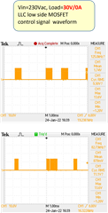
In order to find out the cause of the high frequency noise from LLC transformer, I have measured the control signal of the low side switch under no load, 10% load (0.6A), 50% load (3A) and 100% load (6A). Measured waveforms are shown below:

no load (Vo=30V, Io=0A)
 r

10% load (Vo=30V, Io=0.6A)

50% load (Vo=30V, Io=3A)

100% load (Vo=30V, Io=6A)

From above measured waveforms, we can see the frequency is not fixed even the input and output are stable. Based on my understanding, the LLC is using frequency control method to regulate the output. So the switching frequency is different while the input voltage or load is different. However, during the test, the input voltage and the load are both stable (230Vac from AC PSU, 400V DC bus from PFC stage and output connected to DC electronic load), but the switching frequency is varying very fast. Is there something wrong?

I am thinking maybe the problem is from the feedback compensation loop? or the wiring of the transformer (I didn't solder the transformer on the board, the modified board photo is shown in the other article)? I am hoping to eliminate this high frequency noise. Could you kindly give me some advice? Any opinions and suggestions are welcome and appreciated.

Many thanks.

  • Hi Sean,

    The converter is clearly operating in the burst mode. 

    During the burst mode (or in normal mode), the frequency of operation depends on the Vcomp signal and VCR feed back capacitor values.

    In the above figure, for example from t5,  you can see that, frequency in a burst packet is changing.

    So, there is no issue with your compensator. Otherwise output voltage would not have been regulated during the light load.

    Light load efficiency is impacted by the components you chose for the power stage. So, you need to optimize the components that you have used for both PFC and LLC power stages.

    From controller point of view, you can try increasing the burst mode threshold value. This would reduce the LLC burst operating frequency also the audible noise. However, it will increase the output voltage ripple. 

    You can also varnish the transformer to reduce the audible noise.

    Regards

    Manikanta P

  • Hi Manikanta,

    Thank you for the detailed explanation. I have two questions regarding the burst mode below:

    Firstly, the control signal during the burst mode is not continuous as shown in the picture you provided. for example, control signal only works continuously between time interval t0-t1, then stops working between t1-t2. But from my measured waveforms, this operation only happened during no load condition. The working interval and non-working interval are very clear. Then the control signals during 10%load, 50% load and 100% load are continuous, there is not a non-working interval. The issue is switching frequency is no stable/fixed while input and load are both stable without any change. due to these, is my converter still working in the burst mode? 

    Secondly, I still have a concern regarding the light load efficiency.


    Based on my understanding, the burst mode is used to improve the efficiency under light load condition. From the above test results, left curve is the efficiency of the original board (O/P: 12V/14A), and the right curve is the efficiency of the modified board (O/P: 30V/6A). We can see the light load efficiency of the modified board is much lower than the original board. So will it become worse if I increase the burst mode threshold value?

    Any opinion and advice are welcome and appreciated. Thank you very much.

  • Hi Sean,

    At no load, converter is clearly operating operating at burst mode where as at all other loads, I am not sure whether converter is operating at burst mode or not. Could you recapture the same waveforms by taking lager time scale.

    If the converter is not operating in burst mode, for a given input voltage and a load, frequency should be constant.

    You need to change the BMTH/BMTL threshold values if you want to operate the converter at burst mode at 10% of the rated load.

    Please refer following e2e post that discusses setting BMTH/BMTL thresholds based on the burst mode requirements:

    (+) UCC256404: UCC256404 won't enter burst mode - Power management forum - Power management - TI E2E support forums

    "In order for the controller to drop into burst mode, the FBreplica signal needs to drop below the BMTL threshold. Normally what works for me is to load the converter to the point at which I want to have burst mode, look at the peak to peak voltage on the VCR pin, and use this value to set BMTL on the controller. This typically can get you pretty close and then you just need to dial in the BMTL threshold a little bit more to get it where you want it. The excel calculator should be able suggest a value for the LL/SS resistors once you have the BMTL voltage you want to target (since you are using BW option 6 do BMTH=BMTL/0.6 to get the BMTH level to put into the calculator)"

    Once you operate in the burst mode, converter efficiency should be improved at lighter loads.

    Regards

    Manikanta P

  • Hi Manikanta P,

    Thanks for your suggestion. I have tested the modified board again and measured some new waveforms.

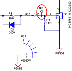
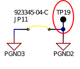
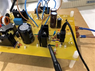
    Firstly, I would like to show how I measured the LLC low side control signal. From the schematic in the user guide, I measured TP4 and TP19


    Then here are some waveforms:

    no load (Vo=30V, Io=0A)


    10% load (Vo=30V, Io=0.6A)

    50% load (Vo=30V, Io=3A)

    100% load (Vo=30V, Io=6A)

    From above measured waveforms, we can see that the control signal is not continuous and stable under any load condition. It looks like the high frequency signal is modulated by a low frequency (LF) signal. And the LF is increasing while the load is increasing as well. This why people can hear a high frequency noise.

    Moreover, from the control signal under 10% load, I believe that it is not operating in burst mode, so the light load efficiency is very low.

    Do you have any suggestion for these two issues (high frequency noise and low efficiency under light load)?  All opinions and advices are welcome and appreciated. 

    Thank you!

  • Hi Sean,

    Could you also share the design calculator and the schematic with me. Thanks.

    Regards

    Manikanta P

  • Hi Manikanta P,

    the schematic is from user guide. The modification components and calculation tool are below. Thank you.

    Design Note for 30V 5A 150W (WE 24V 8A Tr).xlsx

    UCC25640x Design Calculator Rev4.0_30V 5A 150W (WE 24V 8A Tr).xlsxSLUUC46 PFCLLCSREVM034 User Guide.pdf

  • Hi Sean, 

    It seems the converter is operating in burst mode at all the load conditions. 

    Could you also share VCR, ISNS, Vout, and Vin waveforms (with pk-pk and frequency information of VCR and ISNS also with small and large time scale for each load).

    Have you used FB circuit as it is? I am asking because, TLVH431 maximum voltage across cathode to anode is 20V where as your output voltage is 30V. So, you shouldn't use this device. Have you changed this device?

    Regards

    Manikanta P

  • Manikanta P,

    Thank you for the feedback. I will measure and share those signals next week.

    Regarding the TLVH431 issue, I have checked its specification before modifying the board. So I have already replaced it by ATL432LI-Q1 (High Bandwidth Low-IQ Programmable Shunt Regulator) which has higher VKA (37V). Is it ok?

    Thank you for all feedbacks. They are very helpful for me.

  • Hi Sean,

    ATL432LI-Q1 should be okay.

    Regards

    Manikanta P

  • Hi Manikanta P,

    I have measured waveforms of VCR, ISNS, Vout (30V) and Vin (400V). All of them are measured under 0% load, 10% load (0.6A), 50% load (3A) and 100% load (6A).

    Measurement points are:

    VCR: TP5 - TP19

    ISNS: TP7 - TP19

    Vout: TP21 - TP22

    Vin: TP1 - TP18

    The measured waveforms are listed in the excel file below. Please have a look when you are available. Thank you.

    LLC waveforms.xlsx

  • Hi Sean,

    I think you forgot to upload the VCR and ISNS waveforms (both zoomed in and zoomed out versions). I couldn't find those waveforms in the excel file. Could you please upload those waveforms.

    Thank you.

    Regards

    Manikanta P

  • Hi Manikanta P,

    The VCR and ISNS waveforms are located at left hand side in the first sheet called "Waveform_20220223."

    VCR waveforms are from column A to M.

    ISNS waveforms are from column O to Z. 

    Could you please check again?

    And if any waveforms are not clear,  please let me know, I will measure again ASAP.

    Thank you!.

  • Hi Sean,

    Sorry about the confusion. I could find all the waveforms.

    At the full load (6A), you could see that ISNS is zero and VCR is clamped to 3V for some duration. This confirms converter is operating in the burst mode in all the load conditions.

    Also, during burst on, resonant current peak (ISNS) needs to be constant. However, from your waveforms, I could observe that both VCR and ISNS peaks are varying within the burst on period. They could be due to optocoupler saturation and not having proper layout.

    At first, could you change the VCR capacitor values using design calculator to make sure converter doesn't operate in burst mode. (reduce burst mode thresholds and reduce C2 (lower Vcr capacitor) and increase C1 (upper VCR capacitor)).

    Please send me updated waveforms and updated design calculator as before after making above changes.

    Regards

    Manikanta P