- Ask a related questionWhat is a related question?A related question is a question created from another question. When the related question is created, it will be automatically linked to the original question.

Original question:

Dear Sir/Madam,
I have modified the development board, pear number: PFCLLCSREVM034, to output 30V/6A/180W. The detailed is described in the other article "PFCLLCSREVM034: Modified to output 30V/5V/150W."
The test result is mot perfect but acceptable expect two issue: light load efficiency and high frequency noise from LLC transformer.
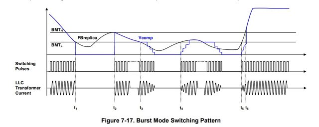
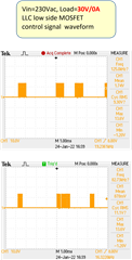
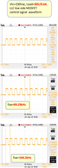
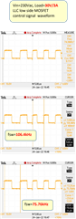
In order to find out the cause of the high frequency noise from LLC transformer, I have measured the control signal of the low side switch under no load, 10% load (0.6A), 50% load (3A) and 100% load (6A). Measured waveforms are shown below:
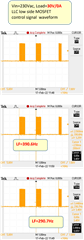
no load (Vo=30V, Io=0A)
 r
r
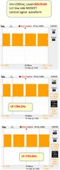
10% load (Vo=30V, Io=0.6A)
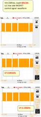
50% load (Vo=30V, Io=3A)
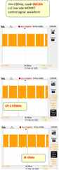
100% load (Vo=30V, Io=6A)
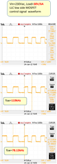
From above measured waveforms, we can see the frequency is not fixed even the input and output are stable. Based on my understanding, the LLC is using frequency control method to regulate the output. So the switching frequency is different while the input voltage or load is different. However, during the test, the input voltage and the load are both stable (230Vac from AC PSU, 400V DC bus from PFC stage and output connected to DC electronic load), but the switching frequency is varying very fast. Is there something wrong?
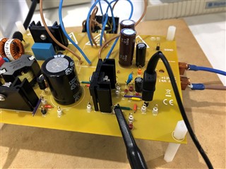
I am thinking maybe the problem is from the feedback compensation loop? or the wiring of the transformer (I didn't solder the transformer on the board, the modified board photo is shown in the other article)? I am hoping to eliminate this high frequency noise. Could you kindly give me some advice? Any opinions and suggestions are welcome and appreciated.
Many thanks.