This thread has been locked.

If you have a related question, please click the "Ask a related question" button in the top right corner. The newly created question will be automatically linked to this question.

TPS22810: Misuse the input and output

Genius 3870 points
Part Number: TPS22810

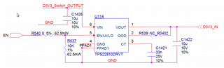
hi there, we found a mistake in SCH design. The output pin1 is connected to input Power D3V3_IN, and pin6 is used as output.  Downstream load of D3V3_Switch_OUTPUT is an MCU, less than 200mA current.

Will this be a problem?  I think this should be OK... but not very sure.

PCB are already  manufactured, we do not hope to do hardware revision. Thanks!

  • Hello Div,

    There are multiple problems with having the input and output reversed. 

    1. QOD will provide a path to ground from the input when the device is disabled.

    2. You will not be able to disable the device, it will at least be D3V3_IN - Vf. 

    3. The internal body diode is not stress tested and it's not guaranteed to hold 3A continuous current.

    With 200mA it shouldn't be an issue with damaging the internal body diode though.

    Regards,

    Kalin Burnside

  • hi Kalin,

    1 and 3 should be acceptable.

    But for 2, do you have information of Vf of the internal body diode? Thanks !

  • Hello Div,

    We do not have any specific data on the Vf range as the device is not meant to be used bidirectionally. You could run tests on the EVM to get an idea, but over a significant amount of devices there would be some variance. 

    Regards,

    Kalin Burnside