This thread has been locked.

If you have a related question, please click the "Ask a related question" button in the top right corner. The newly created question will be automatically linked to this question.

TPS51916: DCAP-2 Calculations and Advice that is not in the Datasheet

Part Number: TPS51916

Hello TI Support Team,

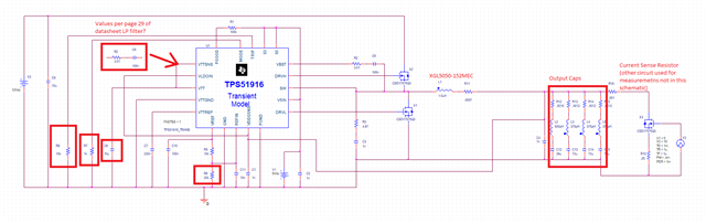
I am using the TPS51916 in a DDR4 application (1.2V) in DCAP-2 mode with tracking discharge - Mode 0 (using 1kOhm resistor at R7 in schematic photo below). Targeting 6.5A as my limit of the output current.

When picking R1 and R2 for DCAP-2 mode, should I just use equation 6 from the datasheet with 0-ESR? That gets me 20K for my application and matches Webench.

The Rtrip calculations come out to about 12K, but simulations in PSpice seem to indicate that 10K will be closer to the 6.5A limit. What would be TI's take? No damage should occur above 6.5A, but I will start to hit the 10% inductance drop of the selected inductor. I honestly don't even expect to see more than 4.2A. 

Is there a target corner frequency for the low pass filter mentioned in the Layout Guidelines on page 29? I am certain that my ESR of the VTT output cap (C8 in the photo) is >2mOhm. 

Would TI have an issue with the use of the XGL5050-152MEC inductor from Coilcraft, and would the output capacitance shown in the photo suffice? I have used Murata's simsurfing to get the voltage derating and paracitics for my output caps in order to be a bit more accurate... They are a 47uF and 3x 100uF X5R caps. Wide temp range is not a major concern.

Thank you,

Donald Weaver

  • Hello Donald, here is my comment about your design:

    1- The output voltage VDDQ has a DC level equal to REFIN (pin 8) and an AC ripple. The DC level is a function of the 1.8V reference voltage VREF (pin6) and the voltage divider R4 and R5 according to the circuit in figure 39. The datasheet calculate R2 in reference to figure 36. Equation 6 is not correct and R1 is missing from the formula. The correct formula is VDDQ = VREF*R2/(R1 + R2) + IIND(ripple)*ESR/2 (referenced to figure 36).

    2- The pull down resistor, from MODE pin19 to GND, 1K from MODE pin19 to GND is for DCAP2, switching frequency 500KHz and tracking.

    3- I double checked, in the datasheet, the overcurrent trip equation 9 and is correct. For 6.5A OCL, 12V input, 1.2V output, 500KHz switching frequency, 2mOhms On-resistance and 1.5uH inductor, the calculated trip resistance is 9.2K. Trip resistance of 10K is good for 6.5A OCL counting the inductor and ON-resistance change over-temperature

    4- There is no concern about the output inductor and the capacitance

    5- I think 10uF/2mOhs is OK 

    I hope this answered your question and please let me know for further support.

    Regards 

  • Hello Mahmoud,

    This answers most of my questions. I have no further concern with items 1, 2, 3, and 4. 

    For item 1, I guess that the very low ESR (1.5mOhm) of my output caps will simply make the IIND+ESR term negligible. I think that is resolved.

    For item 5, My present capacitor selection is actually 2x10uF: GRM155C80J106ME18. These have an ESR of about 5mOhm, which is >2mOhm note... Even when I think about them in parallel. Would this real configuration require the LPF?

    Thank you for your help and time!

    Best Regards,

    Donald Weaver

  • Hello Donald,

    Sorry for the delay! I was out for personal reasons. I would suggest to add a 0.1uF to 1uF decoupling cap at VTTSNS. 

    Please close this thread as resolved and let me know for further support.

    Regards

  • Thank you, Mahmoud!

    I appreciate the quick support once you are back in office. This should resolve my issue.

    Thank you,

    Donald Weaver