This thread has been locked.

If you have a related question, please click the "Ask a related question" button in the top right corner. The newly created question will be automatically linked to this question.

TPS54233: how much minimum input voltage is required for output 3.3V , 1A

Part Number: TPS54233
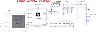
Other Parts Discussed in Thread: TPS54332

Dear All,

My design requirements is

Input : 5V  and output  : 3.3V, 1A

 In my design I have used TPS54233  to generate O/P 3.3V,@1A. Is input voltage 5V sufficient for generating output 3.3V ? please find the attached schematic diagram and suggest.

  • Hi Sreehari

    The schematic looks good. For the application, the Vin is a little bit low, but it can work. The risk is the boot UVLO, so I would recommend to use a higher input voltage like 6V or to enlarge the boot cap value to 470nF or even larger.

    BR

    Ruby

  • Hi Ruby    

    Thank you for suggesting.I have a small doubt, on what basis you have decided the value of boot cap as 470nF, can you please share me the details of calculation of boot cap so that I can understand clearly and move further.

    Best Regards

    Sreehari

  • Hi 

    Ruby will reply you next Monday

    Shuai

  • Hi Ruby ,

    Please update.

  • Hi Sreehari

    Sorry for the long time delay. 

    The design of the boot cap value is associated with the BOOT UVLO threshold, Vin and the gate charge. When we choose the cap, we should guarantee that during the high-side FET on time, the voltage of the boot cap should not drop below the BOOT UVLO. Usually, We would like to choose the voltage of the boot cap would not drop 1% or even lower during the on time. We can use Qg=Cboot*Vdrop to work out the value draftly but it cannot be that accurate (Qg is the gate charge needed for the high side FET on, Vdrop is the voltage drop of the boot cap to charge the FET). Since we should also consider the diode cap and the parasitic of the inductor.

    The datasheet gives the value for typical applications. But when Vin is low, the internal Vcc to charge the boot cap is lower than that with Vin=12V. Another point is that, the duty cycle is 3.3/5=66%, and the load is 1A (some voltage drop across the high side Rdson), which means that the high side FET should be turned on for a long time. This makes the application have a risk to trig BOOT UVLO. 

    I once met a case in which the input voltage is 5V and output voltage is 3.3V, load current is hundreds of mA and the boot cap is 100nF. In this case, the customer met the BOOT UVLO issue (defective rate 3%). They used TPS54332 which is also a 28V device. But they did not meet the issue before because they changed some devices in the BOM such as the diode. I tested 100nF+47nF for the boot cap in the lab and it still had the issue, and I used the 220nF for this application, it could work. To avoid the issue, finally, we suggested 470nF for the application.

    This case is for your reference.

    Hope that helps.

    BR

    Ruby

  • Hi Ruby,

       Thanks for great support.

    Now I can understand clearly.

    Regards

    SreeHari