This thread has been locked.

If you have a related question, please click the "Ask a related question" button in the top right corner. The newly created question will be automatically linked to this question.

UCC28064A: Not working in low input voltage below 200VAC

Part Number: UCC28064A
Other Parts Discussed in Thread: TIDA-010015,

Hi,

We are using TIDA-010015 design for 500W power supply design.

We are using LLC IC :- UCC256402A  & PFC IC:- UCC28064A.

We tested only LLC Stage with input 390VDC and Iout 20A. No issue occur.

But testing with PFC+LLC there are issues observed are below

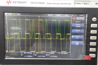
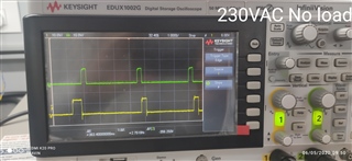
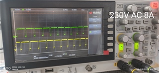
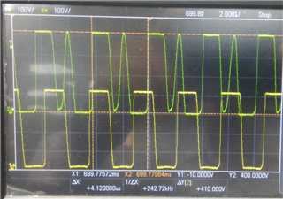
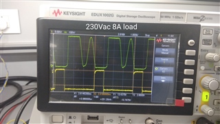
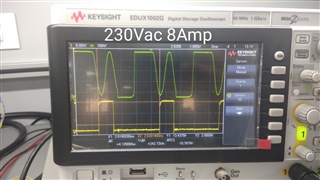
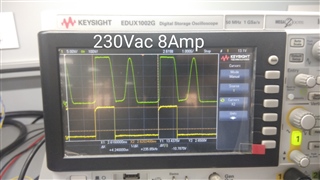
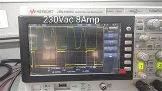
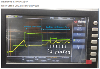
1) If Input voltage 230VAC or above applied and output current 20A applied SMPS working properly.

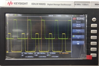
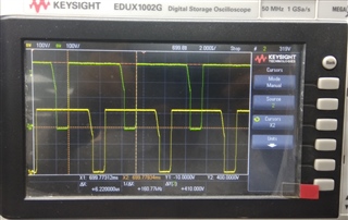
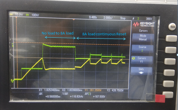
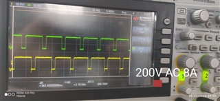
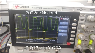
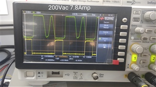
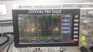
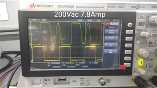
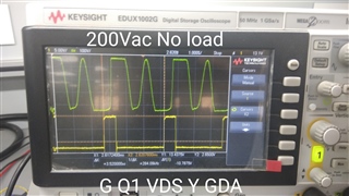
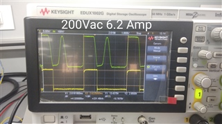
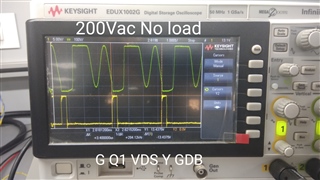
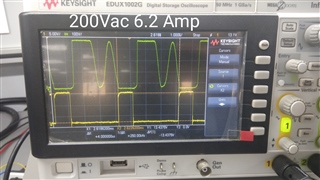
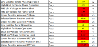
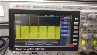
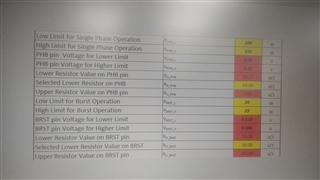
2) But we are testing on lower input voltage below 200VAC, SMPS properly working upto 8A current.

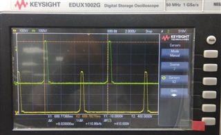
Not able to take above 8A current. Going in hiccup mode on above 8A.

We tried with PFC IC CS pin shunt resistance decrease but no effect of this.

Expecting experts comments here to solve this issue. 

Regards,

Vivek

  • Hi Vivek,

    This is an interesting issue. If you share your schematic (and a completed UCC28064A design tool calculator: www.ti.com/.../sluc645), include waveforms with VINAC, COMP, ILA, ILB at 230Vac @8A and 200Vac @ 8A, I can help you more.

    Other than that, you can confirm proper assembly of the component values that are used for parameters affected by input voltage such as R21/R23/R33/R88 (from TIDA-010015) which would affect brown-out threshold as well as Ton and confirm Rtset value (R89 from TIDA-010015) which may limit Ton at low VINac.

    Regards,

    Ray

  • Hi,

    Schematic same as TIDA-010015.

    Completed UCC28064A design tool calculator - No options in insert tab to attach XLSX File.

     waveforms with VINAC, COMP, ILA, ILB at 230Vac @8A and 200Vac @ 8A

    -  I will check and revert.

    Other than that, you can confirm proper assembly of the component values that are used for parameters affected by input voltage such as R21/R23/R33/R88 (from TIDA-010015) which would affect brown-out threshold as well as Ton and confirm Rtset value (R89 from TIDA-010015) which may limit Ton at low VINac.

    - Confirmed. No issues.

    Other 1 issue observed newly LLC Stage Ho Lo switching pulses are 34 which required 16 as per datasheet. 

    Can you help to solve this issue first??

    Regards,

    Vivek

  • Hi Vivek,

    I will tie in our LLC expert to this thread to help with your question on that stage.

    To attach a file, at the bottom of the reply screen, choose the Insert pull-down and select Image/video/file. When the new panel pops up, click on Upload, then you can browse your hard-drive for the file and the click OK.

    I will await your uploads for the PFC.

  • Hi Vivek,

    The number of pulses in a burst packet depends on the FBreplica signal, BMTL threshold.

    As you can see in above screenshot, it need not be exactly 16.

    Please let me know if you have any further questions.

    Regards

    Manikanta P

  • Dear Ray,

    Thanks for the help.

    Attached  XLSX completed UCC28064A design tool calculator.

    UCC28064A PFC Design Calculator.xlsx

    Regards,

    Vivek

  • Hi Ray,

    Waveforms with VINAC, COMP at 230Vac @8A and 200Vac @ 8A are attached below.

    ILA, ILB not possible to capture due to current probe not available.

    230VAC @8A

    Yellow CH1 is COMP, Green CH2 is VINAC

    200VAC @8A

    Yellow CH1 is COMP, Green CH2 is VINAC

    Regards,

    Vivek

  • Hi Vivek,

    Thank you for the waveforms and design calculator.  Nothing stands out that would result in the issue you're experiencing. 

    1) If you don't have a current probe, hopefully you can show VDS of Q1 and Q12 at 230Vac/8A. If you only have one high-voltage probe, you can just capture in two different scope shots.

    2) Please share your schematic

    3) Please include the MOSFET part number

    4) Can you explain why you chose a 235uH inductor rather than 150uH used in TIDA-010015

    Thank you,
    Ray

  • Hi Ray,

    1) VDS of Q1 and Q12 at 230Vac/8A waveforms attached.

    2) Please share your schematic - Can you share me your mail ID. We don't want to express in forum due to confidential information.

    3) Please include the MOSFET part number - LLC Mosfets :- IPB65R150CFDATMA1. PFC Mosfets:- IPA60R120P7XKSA1.

    4) Can you explain why you chose a 235uH inductor rather than 150uH used in TIDA-010015 -  If you check forums of TIDA-010015 there suggested to use custom parts from wurth electronics.https://e2e.ti.com/support/tools/simulation-hardware-system-design-tools-group/sim-hw-system-design/f/simulation-hardware-system-design-tools-forum/837369/tida-010015-request-transformer-datasheet-for-tida-010015?tisearch=e2e-sitesearch&keymatch=TIDA-010015# )

    230VAC @8A

    Yellow CH1 is Q1 VDS, Green CH2 is Q12 VDS.

    All are the VDS waveforms, but why there are 5 different types of switching?? 

    Regards,

    Vivek

  • Thank you Vivek.  The UCC28064A is a Transition Mode (TM) controller and the first four waveforms are what I'd expect. The on/off times of the FET are dependent on the instantaneous Vin voltage signal.  If you overlay the VAC signal with the VDS signal, you can observe this variation over a full 50Hz cycle.

    The last waveform with CH1 operating continuously while CH2 indicates that phase 2 is in DCM is the one of interest for your issue.

    1. Regarding the schematic, I will send you a private connection request where you can share the schematic with me, non-publicly. However, I'd like to keep this thread going with information you are comfortable sharing for the benefit of the E2E community.

    2. Going back to your original post where you indicated that you lowered the CS shunt resistance, you didn't say by how much you lowered it. Until the root cause is debugged, please reduce the resistance by half so we can rule out an issue with that block.

    3. Please recapture a signal similar to the last waveform (with the DCM on output 2), but please also include the GDA and GDB signals with your trigger set to GDA rising edge.  Capture these with 8A load at 230Vac and 200Vac and also at 200Vac with no load.

    4. When the issue occurs (typically at 8A ~200Vac), does the output of the PFC droop or does it collapse? A scope shot of a load step showing that may be helpful.

    5. Regarding your selection of the inductor, the 235uH agrees with the calculation in the Design Guide for TIDA-010015. I'm not sure if the 150uH in the reference design schematic is an error or if it was changed after the designer made an empirical judgement on the value.

    Regards,

    Ray

  • Hi Vivek & Pravin, let's continue this conversation here. I closed out the other thread.

    Pravin, while Vivek is OOO, this is where we left things in our private chat (of course, I will not share your schematic here in the public forum)

    Hi Ray,

    1. Regarding the schematic, I will send you a private connection request where you can share the schematic with me, non-publicly. However, I'd like to keep this thread going with information you are comfortable sharing for the benefit of the E2E community. - Schematic Attached.

    2. Going back to your original post where you indicated that you lowered the CS shunt resistance, you didn't say by how much you lowered it. Until the root cause is debugged, please reduce the resistance by half so we can rule out an issue with that block. - 2.5mohm and also try with 0ohms.

    3. Please recapture a signal similar to the last waveform (with the DCM on output 2), but please also include the GDA and GDB signals with your trigger set to GDA rising edge.  Capture these with 8A load at 230Vac and 200Vac and also at 200Vac with no load. - I will capture and send you soon.

    4. When the issue occurs (typically at 8A ~200Vac), does the output of the PFC droop or does it collapse? A scope shot of a load step showing that may be helpful. - Attached waveform for your reference. Vbulk drop directly

    5. Regarding your selection of the inductor, the 235uH agrees with the calculation in the Design Guide for TIDA-010015. I'm not sure if the 150uH in the reference design schematic is an error or if it was changed after the designer made an empirical judgement on the value. - I was tried with 150uH inductance same issue observe with 150uH.

    Discussion Point 4 Waveforms

    Waveforms at 100VAC @8A

    Yellow CH1 is VCC, Green CH2 is VBulk

    So Vivek was going to collect the waveforms from discussion point 3. However, based on the different behavior, the actual conditions may change. I will let you decide which conditions would be most informative. Looking at failing condition and just above or below failing conditions to try to determine what's going on.

    Also, I had noticed a discrepancy in R11 & R37 which Vivek indicated were changed from what the schematic shows. I'm not 100% clear on the values of R11, R37, R39 & R41. Please clarify.

    Regards,

    Ray

  • Hi Ray,

    R11=6K2 ,R37=68K ,R39=100K  ,R41=6K2  

    Wave form will follow by half hour.

    Regards

    Pravin

  • Hi Ray,

    Below are wave forms of GDA (Yellow), GDB (Green) triggered with rising edge of GDA

    Regards

    Pravin Khisti

  • Pravin,

    I'm looking for this behavior of VDSQ1 and VDSQ12 with GDA and GDB added to the scope capture.

  • Hi Ray,

    Below are wave forms as required.

    1) Yellow CH1 is GDA, Green CH2 is Q12 VDS.

    200VAC @ No load                                                                      200VAC @ 7.8Amp  (Above 7.8Amp DCM not observed)     

    230VAC @ 8Amp

    2) Yellow CH1 is GDB, Green CH2 is Q12 VDS.

    200VAC @ No load                                                                  200VAC @ 7.8Amp (Above 7.8Amp DCM not observed)

    230VAC @ 8Amp

    3) Yellow CH1 is GDA, Green CH2 is Q1 VDS.

    200VAC @ No load                                                                  200VAC @ 6.2Amp (Above 6.2Amp DCM not observed)

    230VAC @ 8Amp

    4) Yellow CH1 is GDB, Green CH2 is Q1 VDS.

    200VAC @ No load                                                       200VAC @ 6.2Amp (Above 6.2Amp DCM not observed)

    230VAC @ 8Amp

    Regards,

    Vivek Parab

  • Your values for R39 and R41 seem to be off from the calculated values you provided last week.

    Can you simply use 66.5kΩ for R11, R37, R39 & R41 as is in the TIDA-010015 reference design. Let me know if there is a change in the behavior.

    Thank you,

    Ray

  • Hi Ray,

    Checked with R11, R37, R39 & R41 = 66.5kΩ. No change in actual issue behaviour.

    With above PHB values R39 & R41, GDB not switching (ON) properly upto 10A (240 Watts). Not check above 10A (240 Watts).

    What is PHB setting recommended in Watts?

    When need to GDB switching on is ok (If light load efficiency required & If light load efficiency not required) ?

    Regards,

    Vivek Parab

  • Hi Vivek,

    Thank you for checking the operation with the reference design values.

    20%-30% of rated power is a reasonable level for PHB.  It is also suggested that VPHB is at least 600mV greater than VBRST. For your design,  let's try PPHB_L= 110W, PPHB_H= 125W and PBRST_L = 40W and PBRST_H = 45W.  This will result in R41 = 48kΩ, R39 = 195kΩ, R11 = 16kΩ, R37 = 172kΩ 

    Let me know what the PHB_L/H and the BRST_L/H thresholds are with these values.

    Ray

  • Hi Ray,

    Thank you for information. 

    I have tried with R41 = 48kΩ, R39 = 195kΩ, R11 = 16kΩ, R37 = 172kΩ. But upto 100VAC  6A (144W) GDB switching not started (Not checked above 6A).

    Below waveform for your reference.

    Below some more information for debugging.

    Now we are tested with our schematic values and PHB & BRST values R11=6K2 ,R37=68K ,R39=100K  ,R41=6K2.

    Below results observed:-

    1) If 100VAC applied and Iout gradually increased so working upto 21A.

    2) If suddenly 100VAC to 180VAC applied @Iout 9A then goes in hiccup mode.

    So may be issue in startup with load. If Any other protection can there be during startup?

    Regards,

    Vivek Parab   

  • Hi Vivek,

    I'm getting a little confused on the issue at this point, so I think it may be important to take a step or two back so we can re-align. Please answer each question so I can get a better understanding.

    - Has the low-power issue disappeared or have is it just observed to be present only when the load is applied non-gradually?

    - Does DCM still occur as in the 12 waveforms you provided a few days ago?

    - You did not provide the requested PHB_L/H and the BRST_L/H thresholds with the resistor values I provided, is there a specific reason for that? 

    - How did you chose the values for R11, R37, R39 & R41? 

    Note: With the resistor values you just reported ("Now we are tested with our schematic values and PHB & BRST values R11=6K2 ,R37=68K ,R39=100K  ,R41=6K2"), you will have a PHB threshold below the burst threshold (0.34V for Vphb and 0.50V for Vbrst). It is recommended that the PHB pin voltage is at least 600mV higher than the BRST pin voltage. I had chosen ~115W for PHB threshold (1.25V) and ~43W (0.54V) for burst and wanted to see where the actual behaviors occurred.

    - Are you debugging the PFC with the LLC stage disconnected?  If not, please do so and use a bench supply for the PFC-VCC. We don't want any interaction between the two stages during debug.

    Thank you,

    Ray

  • Hi Ray,

    - Has the low-power issue disappeared or have is it just observed to be present only when the load is applied non-gradually?

    :- Issue observed when load applied non-gradually above 9Amp at input voltage range 85VAC to 200VAC. Only at direct power on input voltage.

    - Does DCM still occur as in the 12 waveforms you provided a few days ago?

    :- Yes. latest provided VDS waveforms for reference.

    - You did not provide the requested PHB_L/H and the BRST_L/H thresholds with the resistor values I provided, is there a specific reason for that? 

    :- I have checked suggested values R41 = 48kΩ, R39 = 195kΩ, R11 = 16kΩ, R37 = 172kΩ. But upto 100VAC  6A (144W) GDB switching not started (Not checked above 6A).

    I have checked with R41=33kΩ, R39 = 150kΩ, R11 = 16kΩ, R37 = 286kΩ. PPHB_L= 100W, PPHB_H= 110W and PBRST_L = 20W and PBRST_H = 25W. GDB switching started at 5.9A.

    - Are you debugging the PFC with the LLC stage disconnected?  If not, please do so and use a bench supply for the PFC-VCC. We don't want any interaction between the two stages during debug.

    :- We are debugging with LLC. Because of load not available for only PFC.

    May be issue observed due to output feedback compensation or transient response..Check once at compensation ckt..

    Because we made some changes in compensation ckt so at 100VAC to 130VAC working properly. (Suddenly applied load & input direct power on) but above 130VAC to 210VAC not working going in hiccup mode.

    We checked with C78=10uF from 470pF, R103=5K1 from 10K.

    I am trying to calculate compensation components and I would like to know if you have excel calculator for this part.

    Regards,

    Vivek Parab

  • Hi Vivek,

    The reason I asked about isolating the PFC is because there does appear to be an issue with the LLC stage. From this earlier waveform, you can  the LLC goes into a 1 second "pause" cycle.

    To test the PFC without the LLC, you can use a resistive load on the output of the PFC. Light bulbs for example.

    The compensation component calculations are in the same calculator tool provided at rows 87 - 89

  • Hi Vivek,

    Looks like LLC is operating in fault mode. This can be verified by the looking at the RVCC voltage. 

    Also could you power up the LLC using DC power supply rather than connecting through PFC output so that we can see what's going on.

    Please share the waveforms at the VCR,ISNS, RVCC, LO, Vout, VCC and load current.

    Also could you re-share the updated LLC design calculator and schematic.

    Regards

    Manikanta P