This thread has been locked.

If you have a related question, please click the "Ask a related question" button in the top right corner. The newly created question will be automatically linked to this question.

UCC3895: Errors in datasheet Rev. Q for this part family?

Part Number: UCC3895
Other Parts Discussed in Thread: UCC28951, , UCC2895, UCC28950,

Greetings,

At least one section in this datasheet seems to have been lifted directly from the datasheet for the UCC28951 and does not apply to the UCC3895. 

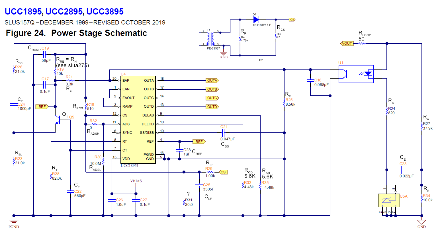
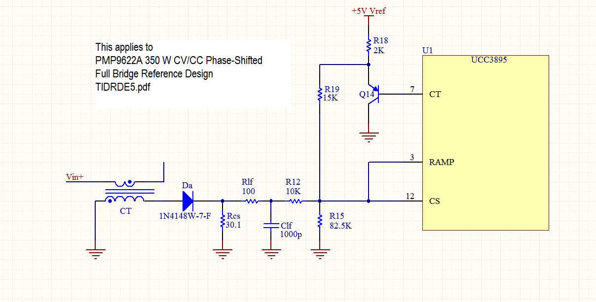
Specifically, Section 8.2.2.10, starting on p. 34, starts out with an error, referring to "current sense signal (Pin 15)", which should say "Pin 12".  It then references an Rlf and Clf which don't appear in "Figure 18. Typical Application" of the UCC2895 document, but do in Fig. 48 of the UCC28951 document.  This section continues with calculations for an R1, R2, R3, and R4 that likewise appear in Fig. 48 of the UCC28951 document but not in the Fig. 18 of the UCC3895 document.

There appears to be an extra "f" in the denominator of Eq. 93.

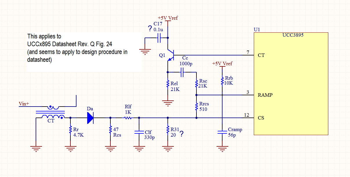
Section 8.2.2.10.6 refers to an Rsc, which is missing from Fig. 18, unless this is a misprint for Rcs?  Resistor Rel and capacitor Cc are likewise missing from Fig. 18.  Meanwhile, there is no information on calculating the values for Rh, Rl, Rslc, Rclamp, etc. around Q1.

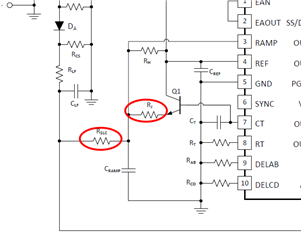
"Figure 23. Daughter Board Schematic" also appears to be misplaced.

I know these devices are fairly similar in operation, and I know that the UCC2895x devices are newer and probably recommended over the UCC3895 family, but it is still very confusing and makes me wonder what other errors exist in this design process.  I'd really like to see an earlier version of the UCCx895 datasheet that has a design procedure that hasn't been corrupted by the apparent "cut-and-paste" from the UCC2895x.  I'm constrained to use this part for various reasons.

Is there any way to provide a correction for these numerous errors?  Would an earlier revision of the datasheet have a correct procedure?  A part this complicated really needs an accurate datasheet design procedure.

Many thanks,

J. Stevens

  • Hello,

    I believe Collin Gillmore may have updated the data sheet based on application note SLUA560 which you can find at the following link.

    You are correct that the information seems to be based on this application note.  https://www.ti.com/lit/an/slua560d/slua560d.pdf

    You should be able to design your power stage based on this information.

    The UCC3895 is an older device and there really was not much design information in it.  It only had equations for setting up the UCC3895.  Such things as timing delays and switching frequency etc...  I believe all of those things are still correct even though the pin numbers in the applications section are off.

    I will notify the Texas Instruments data team of the errors.  It would also recommend using the newer UCC38950 and UCC38951 PSFB controller as well.  There is an excel design tool that goes along with the application note that even includes loop compensation.

    Regards,

  • Thank you for your response.  I have already looked at the EVM datasheet, the UCC28950/1 datasheet, the UCC28950/1 Excel worksheet, and several application notes.  I feel that there is plenty of good information on designing the power stage.

    Right now I'm really confused about the slope compensation circuit surrounding Q1 in Fig. 18 and 24 and the component values calculated in Section 8.2.2.10.6 (all in the UCCx895 datasheet).  Because the UCC28950/1 has internal slope compensation, none of this is addressed in those other resources. Section 8.2.2.0.6 talks about Rsc, Rel, Rrcs, and Cc for the slope compensation circuit, none of which appear in Fig. 18, which instead only shows an Rslc and Rj:

    Is there a correlation between the components discussed in 8.2.2.10.6 and those shown on the example schematics?  Are there are any additional resources for designing the slope compensation circuit?

    I've also been looking at this thread: https://e2e.ti.com/support/power-management-group/power-management/f/power-management-forum/1030835/ucc3895-slope-compensation-circuit, which mostly just makes things more confusing at present.

    I have considered the UCC28950/1 and unfortunately the availability of that part has been very uncertain for over a year now, whereas it is still possible to purchase the UCCx850 (and I have accumulated a number for prototyping before they too disappear).

    Many thanks,

    J. Stevens

  • I figured part of this out. 

    You can't use Figure 18 with the design procedure in the datasheet.  You have to use Figure 24, and reverse-engineer the component names from the component values (e.g. R26 = 21.0k = Rsc).  I added these names to the relevant section of Figure 24 using Photoshop:

    /resized-image/__size/1552x864/__key/communityserver-discussions-components-files/196/Updated-Figure-24.png

    It would be a lot less confusing if Figure 18 was changed to something like the schematic in the link above.

    I also compared three versions of a slope compensation circuit that appear in TI applications literature. First, the version used in Figure 18 of the UCCx895 Datasheet and in the UCC3895EVM-001 schematic:

    /resized-image/__size/1064x613/__key/communityserver-discussions-components-files/196/UCCx895-Datasheet-Fig-18.png

    Second, the version used in the Figure 24 of the UCCx895 Datasheet:

    /resized-image/__size/1208x613/__key/communityserver-discussions-components-files/196/UCCx895-Datasheet-Fig-24.png

    Third, a version used in the PMP9622A reference design:

    /resized-image/__size/1208x613/__key/communityserver-discussions-components-files/196/PMP9622A-schematic.png

    There's also the transistor-less version that you suggested in the thread from 8 months ago mentioned earlier, which I don't entirely understand.  So now I have to figure out which one of these scenarios is going to be the best place to start.

    I found a few more errors in the datasheet Rev. Q: Equations 96 through 101 on p.34 do not apply to this part, and Figures 7 and 8 on p.10 are both plots of input current vs oscillator frequency, and appear to disagree.

    I have a commented/edited version of this datasheet with the errors marked.  If that would be useful, I can send it to you

    Many thanks, 

    J. Stevens

  • Hello,

    I have let the documentation team know that the UCC3895 data sheet needs to be overhauled when the next time the data sheet gets updated.  Thankyou for pointing out the errors in the data sheet.

    The slope compensation circuit in the EVM should have been the same one in the data sheet for the UCC28950.  However, the circuit needs to add half the inductor down slope to the current sense signal to prevent instability.   One of the three circuits you presented should be able to do this.

    The slope compensation circuit in PMP9622A looks like the designer was trying to get more range of out slope comp with an PNP transistor.  This will effect the charging and discharging current of CT and will affect the switching frequency.

    I still think it would be better to use the UCC28950/1 devices instead.  The slope compensation does need all those extra components and may save you money in the long run.


    Regards,