This thread has been locked.

If you have a related question, please click the "Ask a related question" button in the top right corner. The newly created question will be automatically linked to this question.

LM61460-Q1: schematic review and output undershoot

Part Number: LM61460-Q1
Other Parts Discussed in Thread: LM61495, LM61460

hello expert,

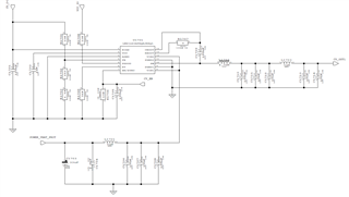
     I am going to use LM61460-Q1 as CV_BUCK in my project, input is battery 9-20V,output is 4-7V,5A max,output load is LED drived by TPS92662.Pls surport the issue below

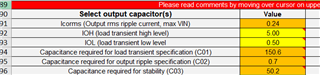
     1.Pls check if the schematic is OK?Is there any suggestion,especially for EMC improvement?And is POWERGOOD signal no used in this case?

      2.when Vin=9V and Vout=7V,the gap is small,will output undershoot happened when the output changed from light load to full load?This may cause flicker of the LED.And how to improve this issue?

  • Hi Zhiyuan,

    Could you fill out the calculator tool and attach it please?

    https://www.ti.com/lit/zip/snvr479

    Thanks,

    Andrew

  • Hello expert,

          Thank you very much for your share.I will check it later.

          Beside, for 61460,is there PIN-PIN product to provide 8A and 10A output? From the official website I only find below  message, but not PIN-PIN with 61460.

          And what is the different between 61460 and the product mentioned in the below picture?

  • I will check.

    -Andrew

  • Hi Zhiyuan,

    The LM61460 and LM61495 have different internals and pinout so it should be treated as different devices. 

    There is currently no p2p device in the LM61460 package that can accommodate 8A-10A. As such please use the LM61495 for higher current converter design.  

    Regarding your schematic, why is there a need to use two inductors? For a 7Vout application, you would only need one output power inductor.

    Regards,

    Jimmy

  • hello expert,

          The 4.7uH one is the power coli of buck.

          And the 1uH one is for EMC inductor of the output Π filter.

          Beside ,about the document you share, why the "Cout" (line 19)keep the same when I change the output voltage ripple(line 8) and the max output current level(line 13)?

         And what is the meaning of C01?I correct my imformation that the output load is LED drived by E522.49(multi channel of CC driver), so the output load may change from no load  to full load.The cal result of C02 is so large.What is the load step slope and the output undershoot in this calculation?

        And what is the meaning of C03?What happen if the Cout is less than C03?

        And is there calculation of the power dissipation of the IC?For worse case where input is close to output, the duty is close to 95%,that the high side MOS is almost always on.From datasheet maximum Rds(on) is 82mR,for 6A application the power will be 6*6*0.082=2.95W, is it too high for the IC?


  • Hi,

    The feedback resistor network that sets the output voltage should be connected to the output after the power coil inductor of the buck. Having another 1uH output EMI filter inductor and capacitor inside the feedback network may impact loop stability. Recommended to rearrange the circuit such that R1701 is connected after the L1702 buck power inductor instead of after L1703 LC filter inductor.  

    C01 is the capacitance needed to address the desired transient response voltage change that was set in Row 10. The larger the load transient step, the larger the output capacitance should be to keep output voltage overshoot/undershoot within the desired specification.

    C03 is the capacitance needed to keep the design stable (usually it is phase margin of around 45deg). This is the bare minimum output capacitance that should be in the design. 

    In your schematic, I would suggest changing your output capacitors C1711 and C1712 to 47uF to just account for MLCC derating. 

    For power dissipation of IC, I would suggest using the Webench designer tool to calculate this value.  

    Regards,

    Jimmy