This thread has been locked.

If you have a related question, please click the "Ask a related question" button in the top right corner. The newly created question will be automatically linked to this question.

TPS55340-EP: TPS55340

Part Number: TPS55340-EP
Other Parts Discussed in Thread: TPS55340

Hi ,

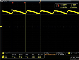
I am currently using TPS55340 in one of my design. Following the specifications. When I am operating IC at low input voltage of 3.6V, I observe input voltage shape change as in below image; Low level voltage is going as low as 2.480V , well below UVLO limt of IC. But there is no dip on o/p voltage of 24V. Why this is happening ?Another observation is , if we increase input capacitor to reduce this ripple, still voltage stabilize at 2.5V only. Whether IC's UVLO circuit is playing any role here. Also, If UVLO is 2.5V, Why IC is not stopped working ? Now when input voltage is falling as low as 2.5V which is well below ICs input voltage range, whether this observation will If we cause reliability issue for IC ?

 If we give external table top Dc supply as input voltage and reduce it to 2.9V, it dips to 2.5V and remain there unless it is again increasing above 3V. Does this observation is because of UVLO pin internal structure circuit ? How really it is controlling this ?

 Vin = 4V to 15V

Vout = 24V, 0.1A

Thanks in advance

Prafulla S.

  • Hi All,

    Can any one suggest me their views on my post ?

    Thanks

    Prafulla S.

  • Hi Prafulla,

    Thank you for using the e2e forum.

    When the input voltage at the TPS55340 falls below the recommended min. value of 2.9V, the IC still tries to operate, but the electrical characteristics are not ensured anymore.
    The reason behind this is to make sure the device does not directly reset if a small transient occurs at a Vin of 2.9V.
    The UVLO should trigger around 2.5V, like you mentioned correctly, so it seems to me the IC is operating right at the edge of not shutting down.

    The voltage dip and ripple on the Vin signal might be explained by the other components on the board (e.g. input capacitors, inductor, etc.).
    Therefore, for further analysis, it might be helpful to look at the schematic of your project.

    Please let me know if you have additional questions.

    Best regards,
    Niklas

  • Hi Niklas,

    thanks for reply. I have one more query. For TPS55340 ( HTSSOP (14) ),  pin no 11 is reserved. It is recommended to connect this pin to ground if not used. can you share the reason for grounding it. What will be consequences if this pin is not tied to ground and kept floating. Do you see any issue in ICs operation in long term ?

    Regards,

    Prafulla S.

  • Hi Prafulla,

    having an pin floating when the datasheet recommends to put it on a certain signal level can lead to unexpected device behavior and worst case also damage the device.

    Best regards,

     Stefan

  • Hi Prafulla,

    I hope you made progress with your design.
    As there has been no additional comments, I will close this thread for now.
    If there are any further questions, please reply below to re-open the thread.

    Otherwise feel free to click on the resolved button.

    Thank you and best regards,
    Niklas