This thread has been locked.

If you have a related question, please click the "Ask a related question" button in the top right corner. The newly created question will be automatically linked to this question.

LM5118-Q1: 12Vin to 14Vout can not provide over 6A output current

Part Number: LM5118-Q1
Other Parts Discussed in Thread: LM5118, , LM5113

Hi Sir,

My customer is developing a board to refer the 4 switch design of LM5118 for 4.2~60V-in to 14V-out with 10A output current.

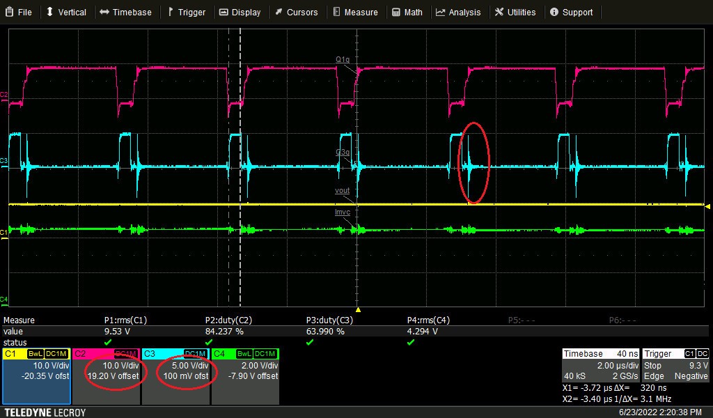
In the boost mode, they would like to test the 10A load for 12V-in to 14V-out, the output voltage will drop when using over 6A load.

Could you please help to review the schematics, I also provided some waveforms for you reference.

LM5118-Q1 schematics:6443.LM5118.pdf

LM5118-Q1 component waveforms:LM5118_14Vout waveforms.docx

inductor datasheet: HFMPD1512-100MA.pdf

  • Hi Henry,

    thank you for supporting the LM5118.

    First of all thank you for the  good report and summary.

    There is one point which confuses me: Then looking through the different plots it looks like the switching frequency has been changed. The fist show ~ 300kHz while the later ones show only 220kHz. Had this been changed during the time the scope plots have been captured?

    Can you please also check the voltage drop across the Q2 and Q4 Transistors and check if one of this FETs gets unexpected hot.

    Can you also probe on the two sides of the inductor.

    Best regards,

     Stefan

  • Hi Sir,

    My customer got low efficiency when the switching frequency was at 300Khz, so we recommend revising the switching frequency down to 220kHz.

    When switching frequency at 300Khz, using 5A load, the efficiency about the 71%; at 220khz, using 5A load, the efficiency about the 80%.

    Can you please also check the voltage drop across the Q2 and Q4 Transistors and check if one of this FETs gets unexpected hot. => The customer informed that L1 gets unexpected hot over 100C when using 6A load. (got the same results at different frequencies)

  • Hi Henry,

    can you please share some of the waveforms you have already captured as mentioned above.

    Also sharing the schematic would be good.

    Best regards,

     Stefan

  • Hi Sir,

    I have provided the all waveforms on the summary report. Do you need us to check which waveforms? we can do that.

    We found some problems shown in the below figure.

    Why the low-side(Q3) mosfet gate power is 5V? high-side(Q1) mosfet gate power is 10V?

    Why the low-side(Q3) mosfet gate have spikes?

    The LM5118-Q1 schematics file: 8764.LM5118.pdf

  • Hi Henry,

    you are right the information - this reply was intended for another thread.

    On the waveform the big disturbance can be seen on the Q3g signals. 
    I assume this is the gate signal of the FET - can you please confirm.

    Can you please also probe this signal together with the output signal of the LM5118 (HO).

    If you check the datasheet of the LM5113 you can see that the source of the Low gate driver (Q3g in your schematic) is the supply of the LM5113 (LMVCC) - this should be 7V.

    The output of the high side driver is generated by a charge pump (with the HB and HS pins of the LM5113).
    To properly open the High side FET the high level needs to be higher then the Drain of the FET - minimum by the Miller plateau + plus some margin ( i would say 3.5 - 4.0 V) - can you check this as well.

    For me it is still not clear if the Inductor gets hot or the MOSFET gets hot and the inductor is the component you will sense it.
    Have you made a thermography (picture with a thermo camera) to find out what is the hottest component on the board?

    Best regards,

     Stefan

  • Hi Sir,

    On the waveform the big disturbance can be seen on the Q3g signals. 
    I assume this is the gate signal of the FET - can you please confirm.

    Can you please also probe this signal together with the output signal of the LM5118 (HO)

    => Please refer to the attached file.

    LM5118_Q1Q3 waveforms.docx

    Could you also check the inductor spec, does it can be used for 4-switch conversion?

    HFMPD1512-100MA datasheet: 7674.HFMPD1512-100MA.pdf

  • Hi Henry,

    for an input voltage of 12V the transformer would be OK. 

    To full confirm can you please give the full input voltage range the system should be working for?

    I am still not sure if the spike on G3q is really there or if this is just a pick up from the probe. How do you measure this? How long the the ground connection of the probe? Are you using a tip and barrel probe setup?

    Can you also let me know under which load condition this scope plot have been made (is this 12V input and 10A load)

    The sequence of the FET switching on and off (without the spike) looks OK.

    Questions for before:

    The output of the high side driver is generated by a charge pump (with the HB and HS pins of the LM5113).
    To properly open the High side FET the high level needs to be higher then the Drain of the FET - minimum by the Miller plateau + plus some margin ( i would say 3.5 - 4.0 V) - can you check this as well.

    For me it is still not clear if the Inductor gets hot or the MOSFET gets hot and the inductor is the component you will sense it.
    Have you made a thermography (picture with a thermo camera) to find out what is the hottest component on the board?

    Best regards,

     Stefan

  • Hi Henry,

    I have not seen an update on this issue for the last 14 days.

    So I assume this issue is solved and I will close the thread.

    If there is something open just reply to reopen with the addtional details.

    To help maintaining the forum it would be good to click the resolved button.

    Best regards,

     Stefan