This thread has been locked.

If you have a related question, please click the "Ask a related question" button in the top right corner. The newly created question will be automatically linked to this question.

BQ76200: mosfet failed during short circuit test

Part Number: BQ76200
Other Parts Discussed in Thread: BQ78350, , BQ76940, TIDA-00792

Hi, 

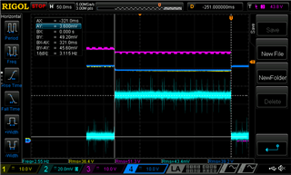
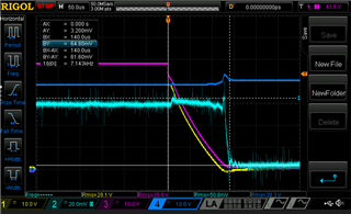
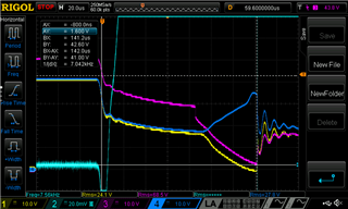
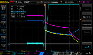
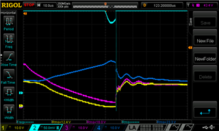
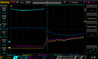
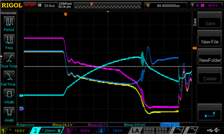
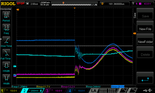
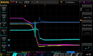
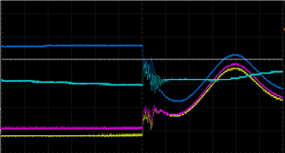
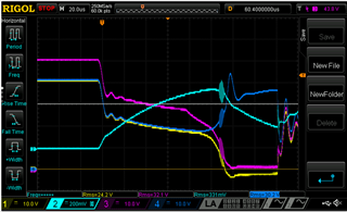
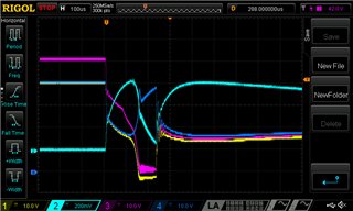
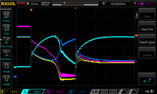
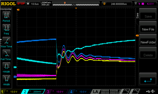
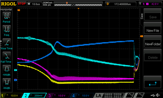
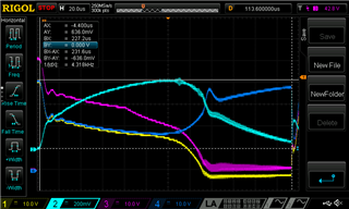
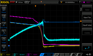
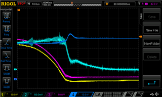
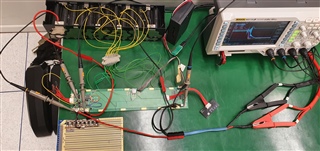
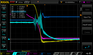
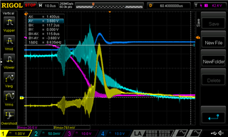
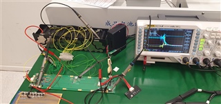
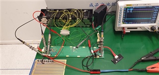
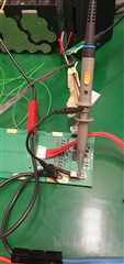
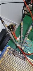
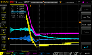
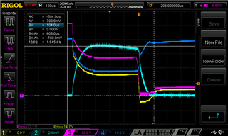
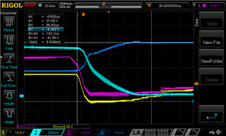
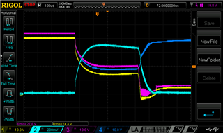
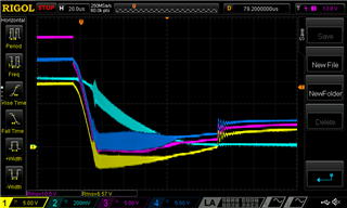
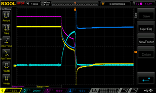
We are testing our design. During testing the hardware failed. One (of two) mosfets failed during a controlled short circuit test on the battery pack. Gate, source and drain are all shorted together. 

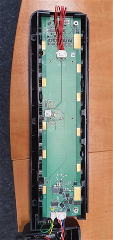
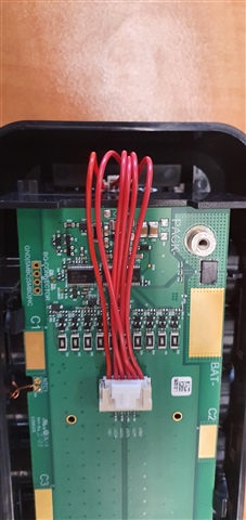
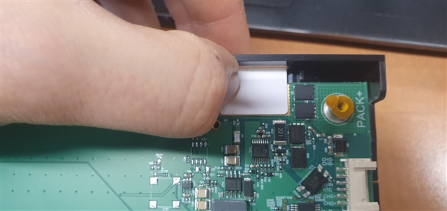
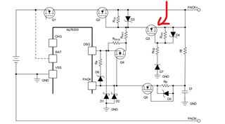
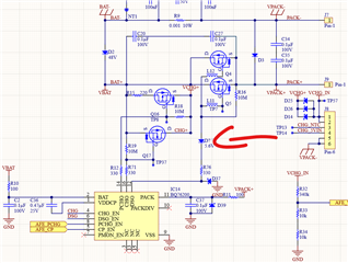
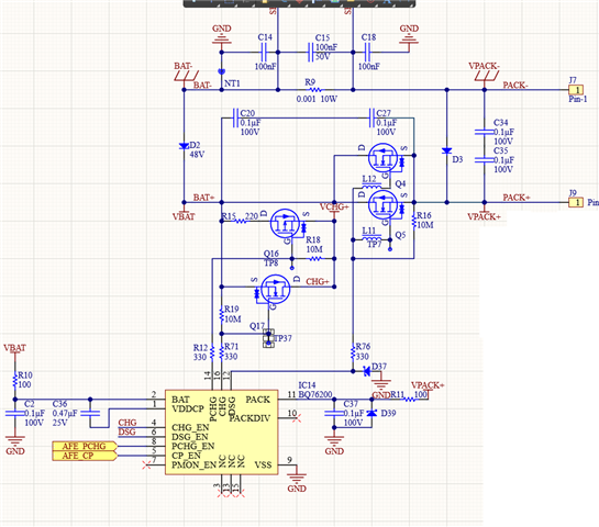
We use two NVMFS6H824NT1G in parallel (Q4 and Q5). After removing the broken mosfet (Q4), we can control the output again, so the BQ76200 doesn't seem to be damaged. We use the BQ76200 in combination with BQ76940 and BQ78350. This is the config file that we use: https://jasa8.dyndns.org/s/WtfRwn59DjbqS39 

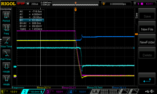
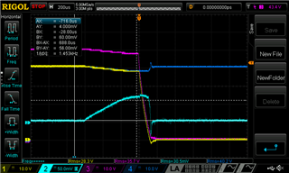
Probably the overcurrent killed the mosfet, but i think they should be capable to handle it for a couple of hunders of µs? Is our timeout to long or should we lower the treshold? Or is the issue related to something else?

Best regards,

Jan

  • Hi Jan,

    I cannot be sure what caused the FET damage in your case, but this thread may be helpful to aid with debug: https://e2e.ti.com/support/power-management-group/power-management/f/power-management-forum/1054353/faq-bq769142-mosfet-short-after-short-circuit-test---voltage-now-always-on/3900591#3900591

    The thread is for a different device which also uses high-side FET drivers, but the advice still applies to this case.

    Best regards,

    Matt

  • Hi Matt,

    That post was very usefull! I do have some follow up questions, we have modified slightly our circuit (==> updated R76 to 2kOhm). Because we noticed a high spike up to 100V when turning of during a overload test (40A), increasing the resistance gave us a better shutdown curve. We tested this up to 65A. You can see the results here:

    Dark blue: battery voltage

    Light blue: current (over sense resistor 1mOhm)

    Purple: Gate voltage

    Yellow (mostly behind dark blue): battery pack output voltage

    When testing a short circuit with this setup the mosfets however failed.

    The yellow signal seems to be indicating that the mosfets are turning off, since the battery pack voltage near the end is dropping but then rises again to 18V. Do you have any insights on what may have caused this issue? The mosfets fail in a shorted state. I don't see a high voltage spike on the drain. 

    Best regards,

    Jan

  • Hi Jan,

    One other thing I noticed in the schematic is that the PACK pin capacitor is too large - it should be 0.01uF. See Figures 16 and 17 in this application report (https://www.ti.com/lit/an/slua794/slua794.pdf ) to see the effect of this capacitor sizing. This could contribute to FET damage in many cases.

    Best regards,

    Matt

  • I see.

    But increasing the resistance also slows down the turn off. I had to do this to avoid the avalanche effect.

    Best regards,

    Jan

  • Hi Matt,

    I did some more testing. 

    I have lowered the resistance again a little bit and did some more measurements.

    Up to 80A the protections work (both AOLD and ASCD). 

    AOLD test at 78A. (same colors as before ==> close to 100A running through the circuit). results are not that much different as before, however there is a short period where a negative current is flowing (at the end of the turn off).


    ASCD test at 56A and 70µs.

    Testing a real short circuit ==> the damping is now slightly better (less oscillating) and you can see the short circuit current dropping (light blue ==> different scale as previous post, so that info may have been lost there). But at a sudden point it fails.


    zoom in on the dropping current:

    You can see here that there is a sudden drop of the current to -70A, is this due to inductive effects after the mosfets have failed?

    Tomorrow i can test with smaller capacitors (must have been a reading mistake when going through the datasheets).

    Best regards,

    Jan

  • Hi Jan,

    I look forward to seeing the results with the smaller capacitor. Hopefully this helps. I'm not really sure what is causing the sudden drop in current, I wonder if the pack voltage transient is larger and faster and is not getting captured on the scope. 

    Matt

  • Hi Matt,

    It is possible that the voltage transient hasn't been captured. I have seen such a voltage peak in one of the previous attempts, but that one failed sooner then this one.

    Jan

  • Hi Matt,

    I have done two new tests:

    -one with recommended capacitor

    -one with recommended capacitor and 4 mosfets in parallel instead of two.

    Both tests failed, however the turn off time was quicker now.

    I only have an image of the second ASCD test.

    this is the moment when one of the mosfets failed.

    I have done also some more AOLD tests, you can see there is a brief moment a lot of noise on the current sense (also vissible on the pack output).

    AOLD testing up to 100A was no problem, but the ASCD didn't work (Isc was approx 600A.

    Do you have any other suggestions to check, measure, ... should i have more mosfets? However i think 4 should be more then enough...

    Best regards,

    Jan

  • Hi Jan,

    Can you tell me the part number for the FETs you are using?

  • Hi Matt,

    I have tested this type:

    NVMFS6H824NT1G

    Normally 2 in parallel.

    Best regards,

    Jan

  • I've also noticed that the pack output voltage (output of the mosfet became slightly negative):

    In the second picture i've added a line to indicate the zero. (between -2 and -4V)

    Or do you think that i haven't captured the moment that the mosfets are failing.

  • Hi Jan,

    I'm not sure. I was just looking through the FET configurations application report (Figure 13 and Figure 17) as a reference point and TIDA-00792 as well. I can't tell if you are capturing the moment the FETs are failing. Here is the link to the report: https://www.ti.com/lit/an/slva729a/slva729a.pdf 

    I was also looking at the FET datasheet and it seems like you are really close to the max current of the FET for this time period. The charge pump capacitor likely needs to be bigger for more FETs in parallel (see Section 6 of the app report for guidance), but I think this would be a problem with charge pump turn-on time, not necessarily with turn-off.

    Other past threads that might provide some thoughts or clues:

    https://e2e.ti.com/support/power-management-group/power-management/f/power-management-forum/674611/bq76200-discharge-mosfet-m7-m11-are-damaged-when-do-short-circuit-with-bq76200

    https://e2e.ti.com/support/power-management-group/power-management/f/power-management-forum/796073/bq76200-bq76200-scd-mos-short

    https://e2e.ti.com/support/power-management-group/power-management/f/power-management-forum/892853/bq76200-fail-to-pass-the-short-circuit-test

    When you replaced the damaged FETs, have you also replaced the BQ76200 IC in case it was damaged?

    Regards,

    Matt

  • Hi Matt,

    I will test again, but it might take a week. with 4 mosfets we we normally can switch up to 400A continously (we don't have the cooling for that amount), but i think that 600A for 500µs shouldn't be an issue, right? currently i use 70µs delay (22A ASCD current). so the expected turn off time should be around 150-200µS? or does it take longer, because obviously our tests fail. I may build a test setup with 6 mosfets, or do you think we need even more?

    I agree, the charge pump cap is more for the turn on time.

    No i did not replace the BQ76200, it is possible that it is damaged. But it seems to react fine, AOLD currents up to 100A are no issue.

    I will have a look at these threads.

    Best regards,

    Jan

  • Hi Matt,

    I have increased the charge pump capacitor to 940nF, the mosfets of my type are 2.5nF, i have used for this test 8 mosfets (on a sperate pcb but still very close to the bms pcb ~3cm max, so it should be ok). 8 mosfets should be plenty for the short circuit test. But however the test still failed.

    ASCD = 67mV(/A), 70µs; total Iscd =~600A.

    I notice that the turn off time is a bit slower, but not that dramatic i think? I have no clue why it fails after ~230µs. previous scd tests failed a little bit sooner (~160µs).

    At this point i have no clue what could be the cause of this. Is there somehow a way i can get additional support to tackle this issue?

    I did one succesful test with ASCD 67A 70µs with a controlled load with a discharge current of 120A-150A, this one was succesful:

    Best regards,

    Jan

  • Hey Jan,

    Matt is out of office until tomorrow. Support will resume then.

    Thanks,
    Caleb

  • Hi Jan,

    I'm not so familiar with this device, but until Matt gets back I took a quick look (it is a long thread, so I haven't digested it all).  It seems probably the thermal load is too high for the FET in that final stage before it blows - the current is still not getting to zero quickly, but you have a huge Vds (30V+) across the DSG FET for 50+us, which may exceed your FET SOA.  It appears that FET can handle 20A for 10us with 30V Vds from the datasheet SOA plot.

    I gather yellow=PACK+, right?  So it seems with PACK+ going negative, even when the DSG gate is ~0V, you have enough Vgs to keep significant current flowing.  Your short is pulling PACK+ toward PACK-, which is around -200mV due to the drop across your sense resistor, but it appears PACK+ is much lower than that, maybe a few volts below gnd.  It also seems to be fairly stable while negative, not like an inductive transient, so I wonder if you have some IR drop along some traces or wires that are causing this voltage drop when the current is so high.  You might also look at where you have your scope ground connected, make sure you're not missing some voltage drop due to how it is positioned.

    Thanks,

    Terry

  • Hi Terry,

    Yellow = P+

    Purple = gate discharge (before filter)

    Dark blue = B+

    Blue = VSense

    Gnd probe is connected to Vsense (B-) not P-.

    At the top right you can see the sense resistor and at the bottom right the high side switch. The power traces have been kept as short as possible. But for the test setup the battery b- and b+ have both 20cm (wires to the bms => pack and bms are separated). I have no photo of the test setup at this moment.

    By default the pcb has 2 mosfets. The load (short circuit) is attached to the screw terminals (so also some wires). Voltage drop may be happening indeed. I have to examine the results more in detail. But here you have some photos to give you an idea about the layout.

    Best regards,

    Jan

  • Hi Terry and Matt,

    I have taken some pictures of my setup (see below and at the end of my post):

    As you can see, the ground clip is connected to B- on the BMS, and on P- a probe to measure the voltage acros the sense resistor. on the left side (screw post) is P+, then there is room for some mosfets. But to test a higher current setupt i have added an external board. and then you have B+. The wires between the BMS are nearly 20cm and 2.5mm² and are just there for easy replacement of broken components for the SC-testing.

    It is indeed true that there is a negative voltage on P+ of 2-3V. But i am not really sure what the cause of that negative voltage is. 

    Test case with a overload current of 120A (protection set to 33A, 320ms).

    Yellow is P+ (zoomed in), you can see that even in this scenario that there is a negative voltage. (the noise on the light blue is not always present).

    I have have also measured the voltage drop accros the wire from B- BMS (gnd clip) to B- battery pack (probe)

    During the overload it is negative as expected (600mV), but when shutting of, this spikes to a positive value... is this what I also see on P+ going negative? Is this related due to the wires I 've used in my test setup?

    setup of the executed measurement:

    Some additional photo's of my setup:

    I haven't done yet a new SC-test, because I'm trying to get some more clarity on the negative P+ voltage. Because it seems right about what terry says. The gate is excited for 2-3V, which maybe increased the cut-off time.

    Best regards,

    Jan

  • Hi Jan,

    The negative voltage on P+ is really strange. I was wondering if you can share the schematic of the bottom side of the circuit - I expect the negative battery terminal is connected through your sense resistor to P-? I think the sense resistors are on the 2nd board, right?

    How are you creating the short circuit condition - is this using an electronic load or some type of switch? Is it possible the load has large inductance?

    Long wires can certainly cause problems with short-circuit testing, but we are having trouble explaining this exact behavior you are seeing. 

    Best regards,

    Matt

  • Hi Matt,

    The PDF contains the schematic of the AFE and high side driver.

    1524.AFE.pdf

    AFC.pdf

    On the right side of the green PCB is the sense circuitry and BQ76940 IC. On the left side is the BQ76200 (high side driver) They are quite a distance apart, but this way the sense resistor could be close to the negative terminals and the switching mosfets close to the positive terminals to limit the amount of power traces on the bms itself.

    I do two kinds of testing with the same device. Overload current testing (configurable up to 120A), which i think is DC-electronic load. The other is short circuit, and it sounds like a switch closing. The documentation of the device is not very clear, but I'll have another look at it. The battery to BMS wires are nearly 20cm i guess. From the bms to the testequipment is longer, but i don't know how much (i cannot check on the inside), but it is easily 50cm or more.

    Best regards,

    Jan

  • Hi Jan,

    I noticed in the 1524.AFE.pdf schematic, the filter resistors are missing from the SRP and SRN pins. I do not think this is causing the problem you are seeing directly, but it would be good to have the filter in place on these pins to avoid false triggering of protections and accurate coulomb counting. 

    I suspect the long wires in your setup may account for some of the strange things we are seeing on the scope captures. It would be good to optimize the test setup to keep wire length to a minimum. The scope probe ground is connected far from the other grounds as well. Differential probes may help for some signals. I wonder if there is large inductance on the DC-electronic load that may be affecting the test too.

    Regards,

    Matt

  • Hi Matt,

    As noticed before the battery pack is between -2V and -5V (in the case of SC). But the DSG pin takes a while to reach 0V. so this means there is a Vgs of nearly 4V. 

    (purple = Vdsg, yellow = P+, light blue = P-/current sense)

    The dark blue line in this case is the GND measured close to the BQ76200. It has a ripple of (-)1V peak when the trigger happens. 


    I am wondering if this might help... However the DSG pin at least should drop to 0V, without the aid of this circuit.

    But according to my calculations if I assume that the voltage drop over D7 is nearly 0.4V and Vgsth is 1.4V I need atleast a negative voltage of -1.8V. which is on the edge. Do you have maybe a suggestion to improve it?

    Best regards,

    Jan

  • Hi Jan,

    I would need to look at this closer. Do you know how much inductance your load has? Have you tried the test with shorter connections - the long wires will create a lot of inductance.

    Matt

  • Hi Matt, 

    I've done some more testing.

    1) i 've used different mosfets, this was a success (tested with 4, 3 and 2 mosfets): AOB290L (see screesnhots below). The main differences i could notice between the original mosfets and this, that his type has a better SOA (safe operating area), and slightly higher Vgs(th).

    2) i've tested again with the original mosfets (8 pcs in parallel) and added a zenerdiode right here:

    With the idea that it would keep the gate voltage closer to P+ (when it goes negative). For some reason this setup works, but i cannot measure a big difference in voltage at the gate (see screenshots below):

    In the first screenshot the dark blue probe is the B+ voltage and the purple probe is the gate voltage at the ferrite bead.

    In the last screenshot the dark blue probe is the gate voltage at the ferrite bead and the purple probe is the gate votlage before the zenerdiode.

    I would have expected that the dark blue line and yellow line would be much closer but still are 2 to 4V apart. But somehow this setup works.

    Here are two screenshots from previous measurements where the mosfets failed:

    I think with adding the zenerdiode i've changed something but not entirely what i wanted to change, but somehow it sort of works.

    What i can conclude of this:

    1) the other mosfets survive probably because they have a higher SOA curve and higher Vgsth and need a higher (more negative voltage to turn on)

    2) with tampering the gate signal i've changed slightly the Vgsth on the original mosfets, keeping them better shut.

    3) the negative voltage is thus probably the reason why it kills the mosfets, because it remains conducting for a little bit.

    The question now is how I can make sure the gate follows the slightly negative voltage so it will keep blocking the current. Because i probably can't get rid of the negative voltage. Do you have a suggestion on how to force it to be at the same level as P+? 

    I do yet have to try the circuit below, but i am affraid that the turn-on voltage for this is to big, since P+ is only slightly negative.

    To answer your question about the short circuit tester. The documentation of the tester is very limited, but it seems to be some kind of a big relay that creates the short circtuit, if it fails the relay opens up after 1s. So all the inductive parts are just the cables from the battery pack and tester.

    Best regards,

    Jan

  • Hi Jan,

    I wonder if your adding that Zener has effectively increased the series resistance between the DSG pin and the DSG gate, and that may be what is helping the most here.  So then I wonder if just increasing the value of R76 may help similarly.  The increased resistance will slow the FET turnoff, reducing the transients, and causing less excitation of the system inductance.  Normally you will need to tune that turnoff to not be too fast (due to inductance effects) and not be too slow (so that the FET is turning off so slowly it exceeds its thermal limitations).  I wonder if you can handle an even larger resistance there before the FET turnoff is too slow for you, you may want to experiment with larger R's and see how it handles those, or do some hand calculations on the FET cap and series R, to see how it matches the FET SOA.  I wonder if you may be able to handle much higher R, such as a few kOhm, and still be fast enough.

    You might be close to the edge where it passes or fails, which is then why the separate FET with better SOA helped too.

    Truly, the photos of your wires appear crazy long.  In testing I've done in the past on the bench, I've had to rewire/solder cells to a board multiple times, squeezing the wiring down as short as possible, to minimize the inductance.

    Thanks,

    Terry

  • Hi Terry,

    I have reduced the wire length to reduce the inductive effects. As soon as i am sure that the mosfets can cope with this situation, then the bms will be mounted directly on the battery pack.

    I don't think I should increase the resistance. I have tested the circuit I wanted to test before now. Where it keeps the gate better shut. 

    Now it can disrupt the SC (111A, 100µs). The turn off time is now about 15µs. But the voltage on Bat+ now surges up to 80V and P+ drops to -30V. 

    I have tested this also with 200A, 100µs, but here it failed again. I think the turn off time is now to short, because the mosfet has no resistor in it's path which causes it to turn off to quickly. However it were not the mosfets that failed, but diode D1 blew up and my power supply, providing power to other parts failed as well. I am not sure if the diode blew up trying to consume all the current when VP+ drops below 0 or because of a voltage spike... The power supply failed due to a voltage spike i think. I am going to add a resistor in that path to slow down the turn off sequence a bit.

    Before this tests I think the gate was not low enough to keep it should fully which reduced the inductive effects ==> very slow turn off. but now it shuts off very quickly killing other parts of the circuit.

    Suggestions are welcome.

    Best regards,

    Jan

  • Hi Jan,

    After you minimize the wiring, then the remaining inductance is in your electronic load and the cells themselves.  You might see if you can rig up another way to do the short without using that same load, in case that is a primary source of inductance.  Then if the cell inductance is significant, you'll need to reduce the turnoff speed of the FETs so that you don't get so much overshoot on the stack when the FETs are disabled.  When it turns off too fast, the stack will rebound much higher, and that high voltage can damage other things connected to that node.

    Thanks,

    Terry

  • Hi Terry, Matt,

    I think my issue has been resolved

    The conclusion for me (bold for most important solutions):

    - SOA of the mosfets is very important (even more if you have some inductive effects)

    - Inductive effects caused the gate to be slightly higher then vgs(th), but this could partially be countered by adding the negative protection circuitry, which keeps the gate nearly at VP+ when driven low.

    - Correct filter caps are needed

    It would be nice if you could confirm that this circuit is ok for this application (since in the application note this is more hightlighted as a protection against an external negative voltage, while in my situation this negative voltage is a cause of the short circuit and inductive effects).

    I'm going to do a series of test with no wires between the battery pack and bms. I will post the results later and marked it as resolved then.

    Best regards,

    Jan

  • Hi Jan,

    I think this circuit should help protect against the negative voltage you were seeing.

    Regards,

    Matt