This thread has been locked.

If you have a related question, please click the "Ask a related question" button in the top right corner. The newly created question will be automatically linked to this question.

UCC2808A-1: half-bridge forward converter power-up issue when dry

Part Number: UCC2808A-1
Other Parts Discussed in Thread: UCC3808-1, TL431

Hello,

I would appreciate if somebody could help me fixing a problem affecting an old design initially based on an UCC3808-1 and now using an UCC2808A-1.

Regards

Gilles

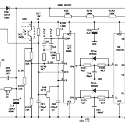
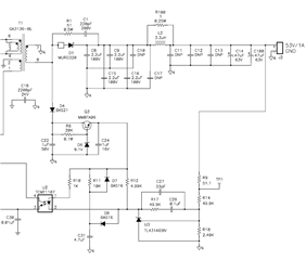
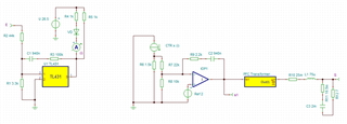
We are using an UCC3808-1 at 200kHz for a half bridge forward converter (400V to 35.8V 8A). See schematic in the attached pdf

WEFA339 H4 - FLAT.pdf
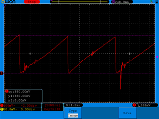
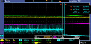
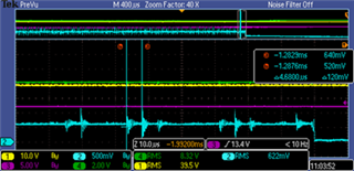
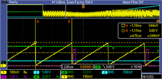
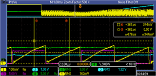
The ramp on the CS pin of the UCC3808-1 is not an actual image of the current but a ramp generated by an RC network.
We had problems keeping this ramp in range due to tolerances affecting the JFET Q40 and then opted to use the UCC2808A-1 which includes an internal FET for clearing the ramp on the CS pin.
The ramp is now in range [0 - 400mV] but some of the units do not start properly when running dry.

Are they any difference in the feedback between the UCC3808-1 and the UCC2808A-1 which could explain the problem?

Transformer:
primary: 20 + 20 turns ~1800uH
35.8V: 8, 8 turns
15V: 5 turns
26.5V: 6 turns

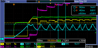
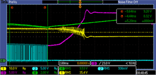
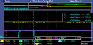
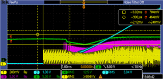
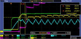
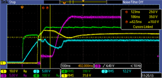
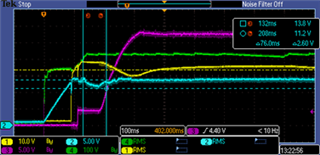
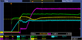
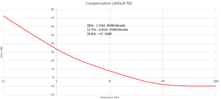
Below is scope capture and a sequence describing the problems:
1) Power-up "400V boost" (CH4) at ~340V
2) VCC (CH2) of the UCC2808A-1 (U12) reaches ~12.5V, the switching starts
3) the voltage on the 35.8V rail (CH1) increases and gets above the set point.
4) the duty cycle on the UCC2808A- 1 (U12) is too small to maintain VCC (CH2) above ~8.5V
5) the switching stops and the cycle restarts at step 2


  • Hi,

    Your attached circuit does not seem show UCC2808A or UCC3808.Please include either into your circuit.

    If your CS is not from the real current sensing, then you need to adjust its magnitude so proper driving pulses can be obtained if you see the driving pulses become too small.

  • The schematic of the supply is in the file "WEFA339 H4 - FLAT.pdf" from my previous post, the UCC3808 (now UCC2808A) is U12 (top right).
    The magnitude on the CS ramp is [0 - 400mV].

    Regards

  • Hi,

    I suspect Q40 Vgs threshold is varying from device to device so Q40 may turn on / off at different R/C to cause different CS voltage . Usually a bipolar transistor can produce better tolerance in such a case. I suggest you use a bipolar transistor for Q40. 

  • How do you control the minimum width of the pulses from the amplitude of the ramp? Is there an easy relationship?
    Up to now I only controlled the maximum width of the pulses when breaking 500mV.  

  • Q40 (J177) is no longer used as the UCC3808-1 has been replaced by an UCC2808A-1 including an internal FET clearing the capacitor connected to the CS pin. With the UCC2808A-1, the ramp on CS is in range [0 - 400mV]. I don't think the problem is to do with the ramp anymore, even if certainly influence the gain.

  • Hi,

    The ramp amplitude is fixed by the IC internal circuit but its ramp is determined by R17 and C24 which also determines the frequency. You can use an oscilloscope to capture R/C pin waveform with different R17 and C24 to check. Its frequency design is based Equation 1 in the datasheet. But if you want to design the ramp with different R17 and C24, then it is better to capture the waveform and adjust R17 or C24 to find.  

  • Please provide CS waveform along with OUTA and OUTB waveform for analysis.

  • Also provide your updated circuit for analysis.

  • Please also provide COMP waveform along with CS waveform and OUTA and OUTB waveform for analysis. Both COMP and CS determine the OUTA and OUTB pulse widths.

  • R17, C24 is just the oscillator ramp set to 200kHz, I have no reason to change the switching frequency. The ramp I had problems with is the one generated on the CS pin by R135, R138, C69 but I think it is now in range [0 - 400mV]. I know the duty cycle gets unstable without ramp generated on the CS pin but I don't know which results I could expect reducing slightly the amplitude of the ramp. I know it should not excess 500mV otherwise I would not be able to get the maximum duty cycle.

  • Hi,

    You also need to know your COMP value then match COMP with CS ramp. Your CS can stay what it is if COMP value can still be adjusted higher. Or you can adjust CS slightly lower to match your COMP.

  • Refer Fig 9 for CS and COMP relationship.

  • Thanks for your reply, that is difficult for me to capture at the same time, COMP, CS, OUTA and OUTB as I only have 2 insulated probes and as they are not shielded they interfere with normal operation of the product.

    Is that OK to measure COMP and OUTA and assume CS is always [0 - 400mV] ?


    Below is a scope capture I did with a battery scope of the signal on CS with the UCC2808A-1, but this area of the circuit is very sensitive.

    I noticed the compensation set on U12 (C68, C88, R130) could help solving my problem. I removed C88 an my unit started. But I am not confident in modifying the feedback on a product which has been used for years. Could you give me some guidance on that? 

  • Hi,

    Do you mean C89 instead of C88 as C89 is in parallel with C68? I cannot find C88. If you change the IC, then your feedback loop needs to tune up. I suggest you to measure the Bode Plots with your old circuit and then change to your new circuit and measure the Bode Plots. If the new Bode Plots are close to the old then your circuit will be ok.

  • I think you can measure two waveforms at a time and send all of them for review.

  • Hello,

    Sorry, my mistake, I removed C89 to reduce the time constant. Concerning the feedback, for me the UCC3808-1 and UCC2808A-1 had the same characteristics and I did not think a change in the feedback was required. I did bode plots of the unit using the UCC2808A-1 and I did not find instability issue: at 1A: phase margin 83°, gain margin ~33dB

    My problem is at power-up when the unit is running dry. I did not success doing bode plot when running dry, I have been told that is because the unit is not in its linear region of operation and bode plots are not relevant in this condition. The problem at power-up is the voltage on the 35.8V rail on which the feedback is connected gets well above the set point which result in reducing the duty cycle to a level not sufficient to maintain the supply of the UCC2808A-1. I have been able to solve this issue by 2 ways: removing C89 or increasing C21 from 22uF to 100uF.

  • Hello,

    Below are some scope captures just before the UCC2808A-1 stops switching at power-up without load.

    OUTA of U12 just before VCC of U12 becomes too low to operate:

    The pulsing rate of OUTA is ~100kHz, the pulsing width is 340ns (seems stable) amplitude ~8.4V. 
    CH1: 35.8V rail, CH2: OUTA U12, CH4: VCC U12, CH3: "output com +"


    COMP of U12 just before VCC of U12 becomes too low to operate:

    The amplitude on COMP is ~640mV, it seems they are cycles for which no pulse is generated on the COMP pin as if a command was skipped (that does the same removing the 20MHz limit on CH2).
    CH1: 35.8V rail, CH2: COMP U12, CH4: VCC U12, CH3: "output com +"
                   

  • Hi,

    the bode plots can only be measured at steady state.

    as you have 4 channels oscilloscope please capture waveforms of COMP CS OUTA and OUTB together and provide them for analysis.

    you mentioned you have circuit change when using ucc2808a so you need to provide the updated circuit.

    if COMP too low is the reason not switching then you need to find why CONP that low.

  • Hello,

    1) The bode plot I sent you was in steady state. I was thinking a problem in steady state could also be the cause of my problem powering-up the unit when dry, but I did not find problems in steady state.

    2) I only have 2 isolated probes and I cannot record COMP, CS, OUTA and OUTB on the same capture especially if I want to trigger when the problem occurs (the PWM chip stops switching). The COMP pin is very sensitive and I did not manage to record it with other channels without disturbing the unit. My best result was measuring it with a battery scope. The signal on CS is a [0 - 400mV] ramp at the same rate as the oscillator.

    My previous scope captures show COMP and OUTA captured on the same event (when the switching stops) even if that is not the same capture.

    3) The circuit has not changed, the PCB is the same, the only difference is now U12 is an UCC2808A-1 and Q40 is not fitted.

    4) You mentioned COMP is too low, what do you mean by this, what should I expect, what can I try.
    Could you give me some guidance to adjust the RC network on COMP?
    Note: the supply of the emitting diode of OC2 is the 26.5V rail which also collapses when duty cycle reduces too much.

    5) I don't think there is a major problem in normal operation. The problem I have is at power-up without any load.
    The voltage on the 35.8V rail gets very high at start-up especially after the PFC has reached its nominal voltage. U12 seems to have no control of the 35.8V when the PFC voltage raises to ~400V.
    Once the PFC voltage is established, the duty cycle to get back to 35.8V gets so low that is not sufficient to maintain VCC and U12 switching. 

  • Hi,

    COMP CS OUTA and OUTB are referenced to the same GND, so you do not need to use isolated oscilloscope probes to take these waveforms.

    But even with two probes, please do the below so I can know their relationship:

    COMP and CS

    COMP and OUTA

    CS and OUTA

    Please capture them at the same time interval during start up.

    COMP = 640mV is very low, if you look at  Fig 9, you can calculate PWM comparator inverting = 0.64V/2.2 = 0.29V, from page 6 of the datasheet CS to COMP to CS offset is typical 0.8V which can be seen as a battery between CS and PWM comparator non inverting. It means, unless COMP increase to make the PWM comparator inverting > 0.8V, OUTA or OUTB cannot have pulses out.

    As you mentioned you have circuit change when using UCC2808A, you need to provide your updated circuit for analysis.

  • Hello,

    I have done some measurements disconnecting the earth of the scope to have COMP, CS and OUTA on the same screen capture.

    I did not manage to trigger when the switching stops, it seems that is when the chip starts up. The duty cycle increases progressively from a small value to the maximum value (I assume that is because there is no 26.5V for the feedback).


  • Hi,

    Please indicate which channel is for which. It looks yellow = CS, purple = OUTA or B, what about the other two channels?

  • Sorry, I forgot:

    CH1: CS, CH2 COMP, CH3 OUTA, CH4 VCC U12

  • Hi,

    Your waveforms look normal. The OUTA pulse width increase is due to COMP voltage increase - COMP has an internal soft start feature.

  • Hello,

    If the driving of the output is consistent with levels on COMP and CS, I come back to the initial problem and the best way to fix it.

    1) At power-up without load, the 35.8V rail can get well above the set point: ~40V with a set point set to 35.8V.
    I have identified 2 possibles causes to this:
    a) the 26.5V rail used for the feedback is turned ON  ~25ms after the power-up.
    b) the PFC voltage is raising to ~400V and the 35.8V rail raises at the same rate.

    2) When the feedback operates, the duty cycle is too low to maintain the supply of U12 in range VCC. VCC and the 26.5V rail drop up to the point the UCC2808A-1 stops switching.

    Below are my main attempts at fixing the problem:

    - enabling the 26.5V rail earlier: no improvement. Enabling the 26.5V rail after the PFC voltage is set-up: no improvement.

    - reducing the time constant on the COMP by removing C89: that allows the unit to start, but the UCC2808A-1 powers-up 2 times before to get to normal operation.

    - increasing C21 to 100uF, this is the capacitor supplying the 15V regulator of the UCC2808A-1: that seems fixing the problem, the UCC2808A-1 gets into normal operation after the 1st power-up.

    I think the best way to maintain VCC during the power-up sequence is probably to avoid the duty cycle becomes too low due to a too high level of the 35.8V rail.

    Do you have any suggestion?

    How can I change the time constant on the COMP pin of U12? 

  • Hello,

    I did some empirical testing to evaluate how the compensation network of the UCC2808A-1 could help fixing my power-up issue when running dry.
    It seems using ~8k2 for R130 and keeping 470nF for C68 and C89 fixes the problem. My plan is to get the bode plots covering the load range [1A - 8A] to check if if gain and phase margin are still acceptable. If the compensation needs modifying, I think limiting the changes to the TL431 compensation network if possible.

    Do you have a better method for changing the compensation network of the UCC2808A-1?


    Is there a difference between the UCC3808-1 and the UCC2808A-1 which could explain why the effect of the compensation seems different?

    Below are the scope captures I did:
    CH1: 35.8V rail, CH2: VCC U12, CH3: "output com +"
    R130 = 1K2                                                                               R130 = 4K7
       

    R130 = 8K2                                                                                R130 = 11K (noisy under load duty cycle probably unstable)
          

    Any advice welcome.


    Note: I am now on vacation and will restart on this problem from the 26/09/22. 

  • Hi,

    As I remember, you mentioned the circuit has some changes when replaced UCC3808 with UCC2808A. That change may have some effect. My understanding is different current sensing signals are on your new circuit and your old circuit. This can affect your feedback loop. So one another way is to compare the two current sensing waveforms to see if you can make them close to each other.

    The CS internal switch addition is the main difference between UCC2808A and UCC3808. Also UCC2808A has wider temperature range.

  • Hello,

    The only change on the variant using the UCC2808A is Q40 is not fitted as not required anymore to discharge of C69. The signal on CS remains generated by R135, R138, C69, the amplitude of the ramp on CS is approximately [0 - 400mV]. On the variant using a J177 for Q40, the amplitude of the ramp is in the same range for samples operating normally but can be a lot higher [150mV - 600mV] on samples getting problems. This seems due to variation in the cut-off voltage of the J177, that is the reason why I though using the UCC2808A with an internal discharge on CS was a safer option. The problem is that some units have instability at power-up with no load. I did not find in the datasheet differences between the UCC2808A and the UCC3808 which could explain that. 

  • Hi,

    please mark up on your circuit with the changes you made and send the marked up circuit to me. It is difficult to follow your wording for your circuit changes and also needs f my understanding correct or not so marked up would be needed to understand your circuit changes.

  • changes from UCC3808-1 to UCC2808A-1.pdf

    Let me know if that is more understandable in the attached pdf file: left original (UCC3808-1, Q40), right modified (UCC2808A-1, Q40 not fitted). 

  • Hi,

    I will review your circuit differences and will get back to you in a day or two.

  • Hi,

    I had a quick review, and would need more review. But it looks Q40 is removed. To find out if the issue is due to the difference with and without Q40, can you please put Q40 back and everything back to the previous, then test to find if the circuit can work like the before? This will help to find a clue how to make debugging.

  • While you do such a check, I will continue reviewing your circuit. If I have new suggestions I will send to you. But you can start this check to put Q40 back and keep the same as before with UCC3808 to see if your circuit can work without the issue.

  • Hello,

    That is difficult for me to perform the test you requested. The unit which has problem is an unit which already had problem with the default fit (Q40 J177, U12 UCC3808-1). 

    The initial reason for which changes were performed on these PSU is a lot of them failed to start with the default fit when manufacturing them with J177 from Calogic instead of Fairchild and U12 UCC3808-1. The identified cause was the ramp on CS being out of range: not starting from 0V and getting greater than 500mV. This seemed to be due to a low cut-off voltage of the J177. Note: the cut-off voltage of the J177 was still in range.

    The first change which has been implemented was to slow down the raising of the ramp on CS by increasing R135 and R138 to 220K: this solved the issue on most of the faulty units but some of them were still faulty.

    The 2nd change was to use an UCC2808A-1 for U12, removing Q40 and keeping 180K for R135 and R138: this solved the problem on most of the remaining faulty units but one unit was still not starting without load.  Increasing R130 on the compensation network of U12 allowed it to start. Note: R130 is 4K7 on the schematic but the actual default value is 2K2, the faulty unit did start properly if using higher values: 4K7, 8K2, 11K. 

  • Attached is a test I did which is the closest to what you requested: I had 2 units a 2022 unit, sample 65 with the new fit UCC2808A-1 without Q40 which failed to start and an healthy 2013 unit fitted with the UCC3808-1 and a J177 Fairchild. I tried swapping the switching options and it appears the problem follows the UCC2808A-1.UCC3808-1 J177 vs UCC2808A-1.pdf

  • Hi,

    Did you try ucc2808 and J177 in the same board of ucc3808 and J177? What is the test result?

  • Hi,

    I had a full review of this thread. I noticed:

    "increasing C21 to 100uF, this is the capacitor supplying the 15V regulator of the UCC2808A-1: that seems fixing the problem, the UCC2808A-1 gets into normal operation after the 1st power-up."

    It looks your previous C21 is 10uF. While you changed it to 100uF, the startup became ok. I suspect two things. One is your current used 10uF for UCC2808 has larger leakage current than the capacitor used for UCC3808. Second is UCC2808 VDD startup current is at higher end while UCC3808 at lower end based on the specs. So you may need to increase your capacitance for VDD to store energy to deal with them. You may try a new UCC2808 to see if 10uF can make startup ok if by a chance this new IC can have smaller startup current. Is it possible you can change C21 to 22uF, or 33uF to see if the startup can be ok?  

  • Thanks for your reply, unfortunately, I am not able to conduct tests on these units at the moment (hopefully by the end of the week).

    Could you confirm the UCC2808A-1 has a larger leakage current than the UCC3808-1?

    Concerning your last reply discussing the value of C21:

    All units fitted with the UCC2808A-1 were units which did not start-up with the default fit: UCC3808-1 and the J177.
    They did not start either with the initial mod slowing down the ramp on CS which fixed the problem on most of other faulty units (R135, 138 220K instead of 180K).

    I have tried different values for C21, 22uF, 44uF and 100uF. Even if the start-up was satisfactory with 100uF, I was not happy with this option as to me that is just hiding a problem: the feedback on the 35.8V starts to operate when the voltage is well above the set point resulting to an ON/OFF phenomenon on the duty cycle. As there is no load on the 35.8V rail, the time required to get back to the set point is slightly long which causes VCC of the UCC2808A-1 to drop below its operating voltage. It seems that increasing the resistor on the compensation network of the UCC2808A-1 results in less abrupt changes of the duty cycle allowing VCC to remain in the operating range during all the time required for the 35.8V rail to drop back to the set point (R130 increased from 2K2 to 4K7 the value on the schematic is wrong). That is where I am at the moment. My initial plan was to increase R130 to fix the power-up issue and to check if gain and phase margins are still acceptable for load in the range [1A - 8A].

  • Hi,

    UCC2808 and UCC3808 both have the same specs for current but the specs are in a range.

    Also the ic unit you are using for test needs to replace with a new one to check so to exclude the one you use has some defect. So try a different unit to find out.

    Basically if 100uF can work it means there is some current at start is relatively large but not sure where it is from so the first try is to use a new ucc2808 to see if different. 

    it would be better you can use your ucc3808 board to test ucc2808 to see ucc2808 can work on your ucc3808 board so to help to see if your 2808 board has additional leakage current from somewhere else.

  • Hello,

    I have recorded the bode plots on an healthy unit using the following variants:
    1) Default fit: U12 UCC3808-1, Q40 J177, R130 2K2
    2) U12 UCC2808A-1, Q40 not fitted, R130 2K2 (configuration to avoid using J177)
    3) U12 UCC2808A-1, Q40 not fitted, R130 5K1 (configuration which allowed a faulty unit to power-up)

    The below table contains my results:

    Load


    1) 3808-1 & J177

    2) 2808A-1 R130 = 2K2

    3) 2808A-1 R130 = 5K1

    7A

    Phase margin

    27.8°

    40.9°

    25.6°

    Gain margin

    28.3dB

    29.5dB

    21.8dB

    Crossover frequency

    1848Hz

    1592Hz

    2629Hz

    5A

    Phase margin

    34.7°

    31.0°

    21.7°

    Gain margin

    32.4dB

    30.8dB

    23.2dB

    Crossover frequency

    1458Hz

    1684Hz

    2777Hz

    3A

    Phase margin

    34.4°

    35.4°

    24.7°

    Gain margin

    31.4dB

    30.1dB

    22.8dB

    Crossover frequency

    1546Hz

    1665Hz

    2831Hz

    1A

    Phase margin

    78.9°

    79.0°

    73.4°

    Gain margin

    34.9dB

    33.8dB

    26.7dB

    Crossover frequency

    637Hz

    713Hz

    1524Hz

    From these results:

    1) It seems there is no noticeable difference between the UCC3808-1 and UCC2808A-1 when using the same compensation network.

    2) The phase margin is not sufficient and increasing R130 from 2K2 to 5K1 brings it even worse.

    3) Some changes are probably required in the feedback.
       
    Could you give me some guidance on how I could better adjust the feedback?

    There are 2 compensations, one local to U12 (R130, C69, C89) and one local to the TL431 (U13).

    Could you tell me how I could determine poles and zeroes of the compensation of U12 U12 (R130, C68, C89) ?
    I did not find help in the datasheet.

    Do you have any method I could use to adjust the compensation networks on U12 and U13? 

    Thanks for you help.

    Regards

    Gilles

  • Hi,

    Your design has so called Type 3 compensator each on U12 and on U13. There are plenty of articles to describe how to calculate the poles and the zeros. For example,

    Designing Type III Compensation for Current Mode Step-Down Converters (Rev. A)

    But if you search the web with "Type 3 compensator calculator" you will get on-line tools to help as well together with explanation articles.

  • Hello,

    Thanks for your reply.

    I would like to get the power for the feedback LED not from the 26.5V rail, but directly from the 35.8V rail in order to get the feedback active asap.

    As the TL431 is specified to 36V I cannot directly swap the 26.5V and the 35.8V. Is there a standard arrangement for using the TL431 with a voltage above the specified range?  

    Thanks for your help.

  • Hi,

    Yes. You will need to design in an LDO such as the circuit of Q3 in the below example where voltage at 54V much larger than 36V of TL431. The Q3 LDO provide a voltage about 9V for TL431.

  • Thanks for your reply.
    I have another question, is there a way to make sure the ton on the UCC2808A-1 never goes below below a certain width even if the feedback is full ? 

  • Hi,

    To make ton stays above a certain width, you will need to design COMP stays above a certain value, so FB has to be smaller than a certain value. In the meantime, CS has to be able to exceed the threshold corresponding to COMP, refer to the block diagram 1.2R and R divider. 

  • Thanks for your reply,

    1) could you give me an example on how I could make sure ton is never going to be below a certain value?

    2) do you have a practical method to set poles and zeroes on the compensators?
    You said our product uses 2 type 3. Is that not 2 type 2?

    3) I have tried to get the feedback LED supplied from the 35.8V rail, that solves the problem of powering-up when dry but a similar problem happens when changing the load from 8A to 0A. How could I bring the feedback faster and increase the phase margin?

  • Hi,

    1. One way is to clamp FB to a value so FB cannot become lower than a value corresponding to ton.

    2. I suggest you to search the web with "Type 3 compensator calculator" and you will find calculation formulas. The below provides an example. If you want to know what Type 2 and Type 3 compensator, you can go to your college text book or also search for Type 2 and Type 3 compensator to learn what they are and how they work

    https://www.ti.com/lit/an/slva352a/slva352a.pdf?ts=1666625716597&ref_url=https%253A%252F%252Fwww.google.com%252F

    3. Your basically need to understand how the compensator work first in order to improve your converter transient response speed. If you cannot get the answer from your web search you may find if any people within your team can help or you may need to take some courses how to design control loop.

  • I think our product uses 2 "type 2" compensators in series, one directly connected to the PWM chip and the other connected to the TL431 as in the below sketch:

    If I am right, the compensation (s1/E) should be like the below chart (amplitude only):

    Is it common to have 2 "type 2" in series ?

    I don't have any accurate model of the transfer function which could help to determine what should be the compensation to get the expected gain and phase margin.

    What I noticed when I did the bode plots (including the corrector) is the phase margin could be quite small at ~1kHz, 3kHz.
    I don't know if I should add a phase boost in this frequency range and if yes, on which compensator.
    I am looking at a practical method reducing the number of test to tune up to parameters of the compensators when the  transfer function is unknown. 

  • Hi,

    Two Type 2 used together is ok. Type 2 has a zero which can boost phase. You need to measure your current bode plots and then to find how to change the zero location. Basically if you move either zero (its frequency) lower, the phase will become higher. This way is used when a transfer function is not known or cannot be accurately known. So each time you change zeros or poles you will need to measure the bode plots to find if the move is on the right direction then adjust and move again.