This thread has been locked.

If you have a related question, please click the "Ask a related question" button in the top right corner. The newly created question will be automatically linked to this question.

TPS548A20: Output voltage trace routing from Load to Regulator Feedback resistors (near Regulators)

Part Number: TPS548A20

Hi,

We are using TPS548A20 to generate 1.0V @ 10A from 12V.

1.0V goes to Load(MPU) from regulator, 

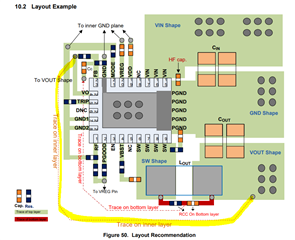
Vout trace which connects feedback resistors(Rtop,Rbot) is coming from Load side in Internal Power plane. This power plane has one side another power plane, other side GND plane both are same distance.

Our part of stackup is

6. GND

7. PWR

8. PWR

9. GND

10. SIG

Whether Vout trace connecting to Feedback resistors should also have solid reference-GND on both sides (we have SIG layers where GND reference is there on both sides) or it can be routed in a Power layer which has GND reference layer on one side only.

  • Hi,

    The FB (and all other sensitive analog traces) must be placed away from high-voltage switching nodes such as SW and VBST to avoid coupling. Use internal layers as ground planes and shield the feedback trace from power traces and components.

    Since you have a solid GND plane between the SIG layer and PWR layer, which can act as a shield, I suggest using via(s) to route the FB trace/components on the SIG layer.

    Of course, you can also route on the PWR layer, but make sure to place the FB trace away from the switching nodes and pour a GND region between them for isolation.

  • HI Tomoya,

    The Feedback trace and its components are near the IC(The question about power trace which is connects to TOP Feedback resistor one end), The source Vout(1.0V) trace is coming from Load in inner Power Layer(Layer 7) which has one side GND or other side another power.

    -----------------------------------------------------------------------------------------------------------------------------------------------------------------------------------------------------------------------------

    Update:

    Whatever you said in previous post, whether it applies to source trace of FB. I was not sure because FB is very high impedance trace and Power trace is opposite..

  • Hi,

    For clarification, I took a screenshot of the layout example from the datasheet. The trace highlighted in yellow is what I'm calling a FB trace. The trace, ideally, needs to go on a different layer separated by a GND plane in between as a shield. However, if it needs to go on a PWR plane, you can still do that, but it needs to be routed away from the high voltage switching nodes.