This thread has been locked.

If you have a related question, please click the "Ask a related question" button in the top right corner. The newly created question will be automatically linked to this question.

TPS65251: Abnormal chip output

Part Number: TPS65251

Hi Team,

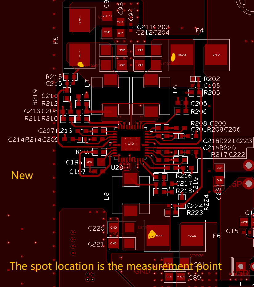
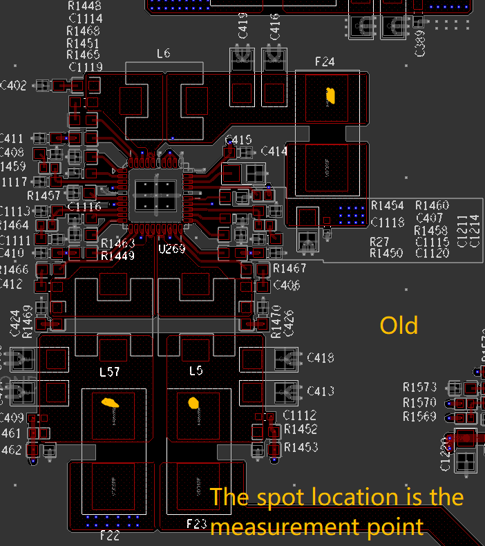
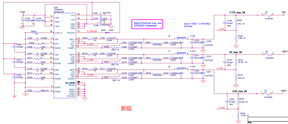
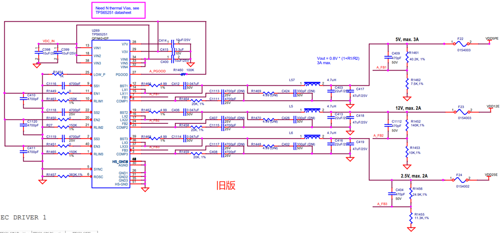
The new design of a motherboard scheme, in which the power part uses the circuit of TPS65251 which has been verified before, but when the board comes back, TPS65251 has no output, the old and new schematic diagram is as follows:

The major failures of the new version are as follows:

The three outputs are 6.9V -0.5V 0.25V, respectively, and the first 6.9V has output only when the fuse is connected. After disconnecting the fuse, all three measurements are 0V.

V3V pin output is 0.25V, V7V pin output is 0.5V, ROSC is about 100mV aperiodic signal

All three EN feet are low (0.2V) and forced up to 3.3V will not work properly.

Modifying the capacitance value of SS1/2/3 has no effect on the results

Replacing the chip has no effect

With the old version test, the old version output and pin status are normal. I don't know where the problem is.

Best Regards,

James

  • Hi Depeng,

    Compared with old version layout, did customer make any changes for their layout in new version board?

    BRs

    Zixu

  • The biggest difference of the new board layout is that the resistance on the ROSC pin is placed on the bottom layer through the via, while the old plate is directly connected on the top layer without via

  • Hi Chris,

    Thanks for your feedback.

    (1) Is there other difference from the schematic and layout? From the schematic, they seem almost the same except the feedback resistors are changed. Whether the resistor connected with ROSC placed on top layer or bottom layer will not cause abnormal output.

    (2) The three outputs are 6.9V -0.5V 0.25V, respectively, and the first 6.9V has output only when the fuse is connected. After disconnecting the fuse, all three measurements are 0V.

    --- When you tested the outputs as 6.9V, 0.5V and 0.25V, what's the position of the test point before you connect and disconnect the fuse? What is the status of all three fuses? Are they all connected?

    Thanks!

    BRs

    Lucia

  • Hi Lucia

    Sorry for replying so late.

    1.There are some differences in PCB layout between the two sets of circuits, as shown in the figure below

    2.The three fuses are not connected, and the first one outputs 6.9V only when the fuse is connected, and about 0.3V when the fuse is disconnected.

    The outputs of the other two fuses are the same when connected or disconnected.

  • FYI,while first output 6.9V,pin ROSC has no output

  • Hi Chris,

    Thanks for sharing the layout.

    (1) I am wondering when you can get 6.9Vout when the fuse is connected, could you please measure the voltage of V3V and V7V and also SW waveform this time? Could you please also let us know what is the loading of 3 Bucks?

    (2) How many new version boards shown this issue? 

    Thanks!

    BRs

    Lucia

  • Hi Lucia

    Thanks for your replying

    1. Whether the fuse is connected or not, the V3V is always 0.2V and the V7V is always about 0.5V.

      The load of 7V is used for the D-pole of nmos (DS load is not connected), 5V is used for the motor driver chip (no motor is connected), and 1.2V is mainly used for the pull-up of some devices. We have a backup solution in the new version that uses other chips, and the backup solution works normally, so I don't think the problem is at the load side

    2. There are three new boards this time,and this problem exists on all the boards

    Looking forward to your reply

    Thanks!

  • Hi Chris,

    Thanks for your feedback.

    The device has two built-in LDO regulators which are 3.3-V LDO and 6.5-V LDO. If V3V and V7V do not have proper voltage, there should also not be proper output voltage. From your feedback, whether the fuse is connected or not, the V3V is always 0.2V and V7V is always about 0.5V, I don't think 6.9Vout when the fuse is connected is a true output. Could you please check below items:

    (1) Check whether all components are mounted correctly?

    (2) Measure waveform of Vin1, LX1, SS1 and Vout1.

    (3) Disconnect R206, R211, R217, try to float EN or use external power supply to enable EN.

    (4) Could you please also send the layout files of new and old version to my email lucia-gao@ti.com? Since the screenshot is not easy to figure out the related components and I want to check other layers.

    Thanks!

    BRs

    Lucia

  • Hi Lucia

    Thanks for your replying

    1. I check the layout and schematic ,and found no device missing, but it is not completely excluded that the device may have resistance and tolerance bit in the process of SMDs 
    2. The voltage of Vin1 has been stable at 15V,and The voltage of Vout1 and LX1 is 6.9V
    3. Once I tried to disconnect R206,and use an external 3.3V pull-up PIN EN1, in this case the V3V voltage was about 1.3V
    4. i goona sent you two layout file to your email later, hoping to hear from you soon
  • Hi Chris,

    My colleague Lucia will give you reply tomorrow!

    BRs

    Zixu

  • Hi Chris,

    Thanks for sending the files. Let's discuss by email.

    BRs

    Lucia