This thread has been locked.

If you have a related question, please click the "Ask a related question" button in the top right corner. The newly created question will be automatically linked to this question.

CSD17484F4: Footprint CSD17484F4 und CSD25484F4

Part Number: CSD17484F4

Hi,

Can you please clarify if the following is true?

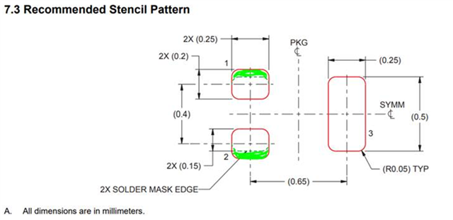
It is recommended to select a "solid mask defined pad (SMD)" (chapter 7.2. on DS) -> ok can be done like this and makes sense, but is usually NSMD.

But in Chapter 7.3. it would be the case that the stencil opening is larger than the soldermask opening; this would mean that the tin is even on the solder mask (see picture below, light green), correct?

Regards,

Gokhan

  • Hello Gokhan,

    Thanks for the inquiry. The recommendations in the datasheet are correct. Please see the FemtoFET SMT guidelines (https://www.ti.com/lit/ug/slra003d/slra003d.pdf) for more details. It is by design to overprint with offset.The solder pad is SMD with 0.15mm to match the component pad. Stencil aperture has to be 0.2mm in order to meet area aspect ratio for good paste printing quality. SMD (Solder Mask Defined) pads are preferred over NSMD (Non Solder Mask Defined) pads to avoid issues due to solder mask registration error when surface mounting FemtoFET.

    Best Regards,

    John Wallace

    TI FET Applications