This thread has been locked.

If you have a related question, please click the "Ask a related question" button in the top right corner. The newly created question will be automatically linked to this question.

LM5122: Bode plot in manual: possible mixup with frequency and rad/s? Where does an output LC filter come in the TF? Feedforward of rectifier ripple? Additional risk of floating ground plane?

Part Number: LM5122

Hi

For this application (a water turbine) I'm trying to convert the energy of of a 3 phase 48VAC PMSG to a stable 80V output with minimal ripple that can be delivered to an off the shelf solar grid-tied inverter (max input 600VDC). The 3 phase power is first rectified, passes some capacitors and is thant boosted by the lm5122 to the stable output. Input voltage can be between 20V and 65V DC, power range is up to 500W. I've got multiple questions from different nature, so if you think that I should split them up, please let me know.

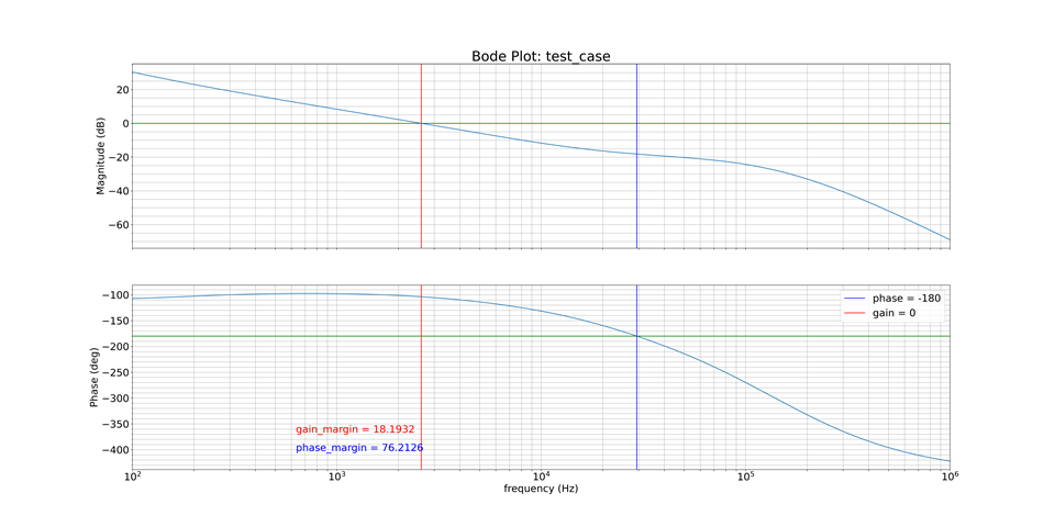
  1. I reconstructed the transferfunction which is given by the manual, but I got a different bode diagram. It looks like my frequency is about 2*pi larger than the one in the manual. Could it be that the frequency in the manual isn't the frequency in Hz, but in rad/s?
  2. The build up of the TF in the manual is a bit too condensed for me to tamper with it by myself so here are some modifications which I would like to simulate:
    1. At the output I have: 8 x 10uF ceramic capacitors and 8 x 100uF with an impedance of 0.17ohm @ 100kHz for each capacitor
    2. I currenctly added an additional LC filter, but I have no clue on how to add this in the transferfunction. The LC filter concists out of 4 x 4700uF capacitors with a tan(delta)=0.2 @ 120Hz and a torroidal inductor of 560uH. How do I add this Lc filter to the transferfunction? This wil for sure reduce my bandwith a lot, but the mayor ripple that need to be compensated is the ripple of the rectifier which is maximum ~70Hz, so I guess this isn't a big issue.
    3. Since I got a ripple in the input, which is high in amplitude, but low in frequency. Could it be an idea to feed forward this ripple to the COMP pin? I see there was a paper about this principlie: https://www.semanticscholar.org/paper/Feedforward-ripple-cancellation-for-a-full-bridge-Jackson-Leeb/2dd41c749d90e4a470947afcdb78d2d58b18152e . I already have a ripple extraction filter, but it isn't that reliable during low rpm's (the 50hz noise than get predominant), but we can solve this with the UVLO by not generating anything when the rpm (=voltage) is too low.  May be this adds too much complexity?
  3. So for the 500W power this setup should be ok. As I look into a larger power range of generators I see that the output voltage of the PMSG inevitably goes up, so the LM5122. The next type of generator will be a 150VAC (203VDC), which is up to 1kW. Any ideas on which strategy / chip would best be followed than to convert this power? I guess control of the high switch will be a problem for the existing range of TI-products, so problably it will be a non synchronous converter?
  4. The solar inverter doesn't like it when the PCB with the Boost converter on is grounded to th earth. It generates an error in the inverter, which would make sense if this was about a damaged wire of a solar panels. So at first I disconnected the ground of the PCB from the earth. During operation I saw that my groundplane pretty fast went to a -200V difference with the earth. This didn't look safe to me, so in order to find a 'way in the middle' I connected a 1k ohm resistor in between the earth and the ground of the PCB. I didn't care about the wattage of the resistor since this floating voltage should only be low power. Now this resistor burned out quite fast. For now I let the ground plane floating: apart from connecting my computer by wire to the controller of the PCB and blowing 200V over my USB, to my grounded pc,  does this involve any more risk?
  • Hello Bram,

    Let me try to answer your questions one by one.

    1. Can you please point me to the manual you are referring to and best to the formula you observe a difference in?

    2a. What question do you have here? My first order estimation would be to add the capacitance and take roughly the lowest impedance as total impedance, but as far as I recall, some capacitor manufacturer have here good material on how the total capacitance and impedance looks like if several caps are paralleled.

    2b. Did you add the LC filter before or after the feedback connection to the device? If it is behind the feedback connection, you do not add this to the transfer function.

    2c. This depends on the needs you have for the ripple on the output and on the converter design. I wonder if it might make more sense to have the LC filter you mention in 2b on the input side instead of having it on the output side? 

    3. I expect that you want to regulate then to an output voltage that is higher than the maximum input voltage. Maybe a boost PFC could be a choice. Please have a look at our reference designs with AC input here: TI Reference Designs Library 

    4. I wonder if there is an issue with the connection of the boost converter low line to the solar inverter. In general for any silicon, it only cares about the voltage difference to its own GND pin, independent of any other difference in the system. But I expect that there is something wrong with some connections as normally there should not be a -200V difference on the solar inverter reference compared to earth ground.

    Best regards,
    Brigitte

  • Hi Brigitte

    Thank you for your quick response!

    1. The manual I'm referring to is the one from the LM5122: https://www.ti.com/lit/ds/symlink/lm5122.pdf?ts=1665403122068& . I replicated the case as given on p36 (typical application). Fig 47 on p43 has a bode diagram. Here I think that the x-axis frequency shouldn't be Hz, but rad/s. 
      1. Part "a)" isn't really a question, more of a background info. Since I didn't pay attention to placing the capacitors before the feedback signal. At the functional block diagram (p12 of the manual), they also place the output capacitors behind the feedback. Also the Webench schematic places the feedback directly behind the switch and before the output capacitors.  Figure 40 on page 35 (typical application) they did place the feedback behind the output capacitors.
      2. The comprehensive forumla regarding the ESR zero en ESR pole on p28 involve low ESR capacitance and "higher" ESR capacitance. Therefor I was concluding that the LC-filter would influence the feedback signal. So to be sure: it is necessary that the feedback signal originates from behind the output capacitors? Or is this only important when an inductor is involved?
      3. placing the LC filter in front does sound easier and less complex than the feedforward option. The LC filter on the end probably needs to stay: the allowable output ripple is not exactly known, since the inverter is made for solar panels, which have only low frequency ripple. So I'm doing the dimensioning of the LC-filter on a trial and error basis
    2.  Yes, Since the input voltage can go to 600VDC from the inverter, the output will always be higher than the input. The pfc controllers do look like a good alternative, thanks!
    3. Yeah, this also looked like a bit much too me, I'll have to look into this, but for now I know that 
  • Hello Bram,

    1. This loop response is measured on the EVM and it is measured in Hz. It seems to be slightly lower than the planned 5.3 kHz, but as not all parasitic components and component variations are considered in the first order calculation, I think this is ok.

    2a. In a real design, it is essential to place the feedback node in the middle of the output capacitors or behind the output capacitors. In diagrams this is often done the way that it is easier to draw. I do not like this approach, but it sometimes makes schematics easier to read. Nevertheless, you should always have the output capacitors as filters between the power stage and the feedback node. If you are not doing this, a lot of noise is injected into the feedback and this can cause the converter to regulate wrongly, oscillate or even get damaged.

    2b. see above

    2c. If you connect the feedback to the IC before the LC filter, it does not have a lot influence on the regulation. If you place the feedback node behind the LC filter, you need to be extremely careful because with 2 LC filters behind each other, in theory you create an oscillator. This means you need to keep the frequencies of the LC combination of the converter and the LC filter at the output far apart, something like at least 1 decade, better more to be able to stabilize the converter. If not absolutely necessary to have a very accurate DC level on the output, then I recommend placing the LC filter behind the feedback node.

    Best regards,
    Brigitte

  • Hi Brigitte

    Thanks again for the response!

    1. I'm sorry, I found some errors in my bode plot. I was a bit sloppy with the 2*pi, don't know why i couldn't find it earlier: 

    3. Those PFC boost converters are actually way better than my current solution. If I understand it correctly, the big difference with a regular boost converter is that the current for a pfc is drawn in accordance with the voltage, right? 

    4. My response wasn't complete: I know I have to look in to this, but for now I know that I can go on. 

  • Hello Bram,

    Thank you for your feedback. Good that you could solve the issue.

    PFC means power factor correction. For high power systems, they are not allowed to draw current out of phase or only peak currents out of the grid. So think about a sine wave signal that shall supply a DC load. First a diode bridge is used to get the negative part flipped to the positive side. Then often a capacitor is used to stabilize the voltage, but this means that only current is drawn when the voltage on the capacitor is below the input voltage which would be just a very short peak at highest voltage. PFC devices make sure that this current need distributes over the full sine wave and therefore draw current that is following the phase and shape of the input voltage. The ones for lower power use DCM, the ones for higher power use CCM (which is a lot more difficult to regulate).

    Hope this short description helps a bit. Please start a new thread with specific questions to a PFC device, if you need detailed help there as my knowledge on these devices is extremely limited.

    Best regards,
    Brigitte