This thread has been locked.

If you have a related question, please click the "Ask a related question" button in the top right corner. The newly created question will be automatically linked to this question.

BQ25306: EMI problems while charging, battery connected via 30cm cable in housing

Part Number: BQ25306

Hello!

We developed a handheld device with the BQ25306 charger IC. The battery is in the housing and connected via a 30cm cable to our PCB. The device also has an LF radio frequency receiver (125kHz). If the battery is charging, especially if the battery is almost full, we see big noise at our LF receiver. This seems to be an EMI problem because if I move the PCB (including the antenna) away from the cable and battery pack everything works fine. The circuit and layout around the BQ25306 is pretty close to your reference design. I tried different things and the best way up to now to reduce this problem was to add an inductivity into line going to battery, see picture:

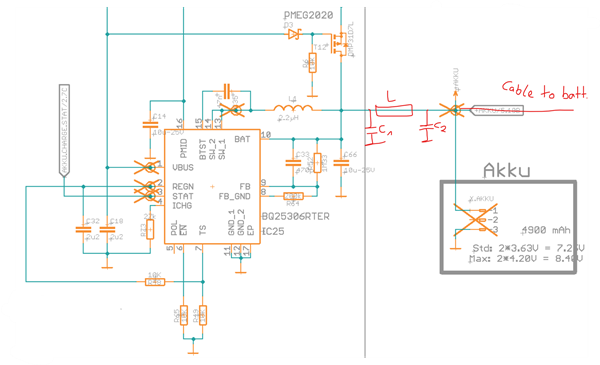
So my question is, is there a problem to add an inductivity L here? How big should this be, I tried up to 10µH? Does the charger work correctly then (up to now it seems so...)? Should I add more capacities C1 or C2? I also already tried a snubber circuit with an R and a C at SW output, with no or only little effect. Do you have other recommendations?

Thanks a lot for your help!

Best regards, Christian

  • Hi Christian, 

    Let me take a look into this and will get back to you in 1 business day. 

    Regards, 

    Arelis G. Guerrero 

  • Hi Christian, 

    Having that LC PI filter before the battery can cause some instability problems with the charger so is not recommended. A few suggestions to improve the EMI are: 

    1. On the layout make sure the decoupling/bypass on PMID is as close as possible to the IC PMID and GND pins with no or minimal vias. This could be the root cause of the EMI problem you are seeing. I would recommend to follow the layout recommendations of the datasheet and EVM.  
    2. Add an RC snubber on SW. An app note on boost converter you can use as reference to get the right empirical values: https://www.ti.com/lit/pdf/slva255
    3. Add a ferrite bead on input not on output. 

    Regards, 

    Arelis G. Guerrero 

  • Hi Arelis,

    thank you for your answer. To your points:

    1. The bypass capacitor on PMID is as close as possible at the IC PMID pin, my design is very close to recommendation in datasheet. As I described, I don't have an EMI problem of the circuit itself, it is the cable to the battery in the housing AND the battery itself. If I bring the PCB near to the cable/battery I see the noise in the 125kHZ LF receiver. I think my "noise" is "produced" after the high side switch.

    2. I will try this again with different values, but my first try was not effective.

    3. I will try this too, but I guess my problem occures behind the high side switch.

    One more question: In the datasheet is written "At certain input and output voltage and switching frequency, the voltage ripple can be reduced by increasing the output filter LC". So maybe it would help to increase the inductivity there, maybe 4,7µH? Or would this be a problem?

    Thanks for your help!!

    Best regrads, Christian

  • Hi Christian, 

    We recommend having a 2.2uH inductor where VBUS_MAX > 6.2V and a 1uH inductor where VBUS_MAX < 6.2V for this device. Giving the noise you are observing increasing that inductor or adding additional capacitance at the output should help. You can refer to section 10.2.1.2 Detailed Design Procedure of the datasheet to make sure to calculate your ripple current, output capacitance based on your charging needs. 4.7uH seems like a good starting inductor selection, and I do not foresee any problem with that value, but is a good practice to test it out on your application as is outside our recommendation. 

    Best regards, 

    Arelis G. Guerrero  

  • Hi Arelis,

    sorry for delayed answer. I have tried several things, but the only one that really helped was to increase the LC output filter (L1 und C66 in my circuit above). I ended up at 15µH and 30µF, increasing capacitance even more would be even better. Do you think there should be a problem with it? In my opinion there should not be an impact on the rest of the circuit regarding stability etc. 

    Best regards,

    Christian

  • Hi Christian,

    The team will get back to you by Monday. 

    Regards,

    Mike Emanuel

  • Hi Christian,

    We cannot guarantee operation with a 15 uH inductor due to the fact that we have not tested with such inductance and it is outside of our recommendation. Increased inductance comes with increased DCR and lower efficiency. Please thoroughly test according to your application.

    Regards,

    Mike Emanuel

  • Hi Mike,

    thanks for your relpy. Ok. Up to now it looks good that it will work, we will test it extensively. Maybe we can reduce the inductance a little bit and increase the capacitance for that. 

    Best regards, Christian Popp

  • Hi Christian,

    Can you please hit "Resolved" to close this thread?

    Regards

    Mike Emanuel

  • Hi Mike,

    thanks for your help, I hit resolved ;-).

    Best regards, Christian