This thread has been locked.

If you have a related question, please click the "Ask a related question" button in the top right corner. The newly created question will be automatically linked to this question.

UCC28810: Power management forum

Part Number: UCC28810
Other Parts Discussed in Thread: TL431, PMP, TLV803

Sir, 

   Ref:, Design No. PMP30882,  We are designing 24V/2A Power Supply using TI's UCC28810 (LED lighting power controller). 

We were able to generate 24V regulated DC output at no load with Input range Vac 135V - 280V. 

We are facing the following issues, so need your support.

1. The output Voltage drops and starts fluctuating between 16 - 20Vdc even on 800mA load. 

2. The Switching MOSFET(IPD70R360P7S) heats up a lot and blows off within a minute.

3. The Output Voltage appears at Input Voltage of 135Vac and not from 90Vac.

An early response would be highly appreciated. 

Thanks,

Subham

  • Hello Ray,

                I observed the Output Voltage at various loads  by reducing the Current Sense Resistance ∼ 10% & then also by 20%, but it had no effect on Output Voltage.

    A) Then I reduced R26 to 610 Ohm & reverted current sense resistor back to original value.. Following are the observations & waveforms:-

    S.No. AC Input Output Volts(V) OutputCurrent(A)
    1 230V 24.23 0
    2 230V 24.22 0.835
    3 230V 24.18 1.545
    4 230V 23.94 2.153
    5 230V 23.42 2.615

    B) Ch1- EA Out

    R26-610 Ohm

    B 1) No Load

    B2) Load 835 mA

    B3) Load 1.54A

    B4) Load 2.15A

    B5) Load 2.61 A

    C) Finally I also observed the waveforms at Ref & K pins of TL 431. Please find below the waveforms:-

    Ch1- Ref Pin TL431

    Ch2- K Pin TL431

    C1) No Load


    C2) Load 835mA

    C3) Load 1.54A

    C4) Load 2.15A

    C5) Load 2.61A

    Regards

    Subham

  • Hello Ray,

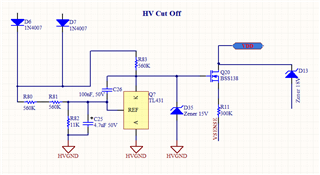
                   In continuation to my earlier queries, I also need your support on the following HV Cut Off Circuit.

    As you can observe I have Integrated the circuit with my existing circuit. The Inputs have been taken from Rectifier Section(Diode D6 & D7) of Vin circuit.

    I have connected the Cut off circuit between Voltage Divider (Res. R11) & VDD.

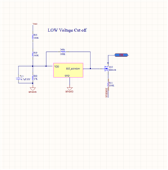
    The following circuit is for Low Voltage cut off with TLV803EA26DBZ, Tried and tested already. Please have look and Suggest some valuable feedback.

    Please advise, will this lead to any operational issues in circuit.

    Regards

    Subham

  • Hi Subham, thank you for the additional information.

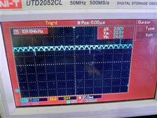
    With the 5ms/div waveforms, I can see that what I had mistaken as "instability" is simply a reflection of the input waveform as provided by the PFC regulation. It is somewhat distorted at higher power, but is relatively as expected. 

    I did notice that your regulation seems to have improved. You are getting a 3.3% drop from no load to full load which is pretty reasonable. What regulation spec do you require?

    That said, I'm looked for other areas that may be causing your output to drop as it does at high load.

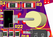
    • The layout, particularly near the output isn't optimal. It's difficult to tell exactly how it will impact the final regulation other than it will not perform optimally. If you need better performance than we can achieve through component adjustment, you will probably need to address the layout.

    • It appears that R6 is a rather large axial-lead resistor. This will result in added inductance on the transformer winding we're trying to clamp. I think you should remove this resistor and put a short bus wire from pin 1 to 2. The diodes should provide adequate clamping.

    • D15 is right near the inductor and power FET, so it is likely heating up. This heating will cause the voltage rating to drop. If it drops more than the the TL431 reference voltage of 2.5V: 24V-2.5V = 21.5V, it will interfere with the output regulation. Check the datasheet on this part and verify that it can provide sufficient breakdown voltage at 100°C and above.

    That's all I have for now. Let me know your findings with regard to R6 and D15.

    Ray

  • Hi Subham,

    I didn't get a chance to look at this. I think it would be more manageable to put this topic in a new E2E thread. I'd like to keep the on-going thread for the regulation and efficiency questions. So if it's not too much trouble, please submit a new E2E question with the relevant info. It will still come to me, so there will be no loss of continuity.

    Regards,

    Ray

  • Hello Ray,

      A) I removed the resistance R6 & shorted its Pin 1 & 2. following are the readings observed.:-

    S.No. AC Input Input Wattage(W) Output Volts(V) OutputCurrent(A) Efficiency(%)
    1 230V 0.46 24.28 0
    2 230V 21.65 24.28 0.794 89.04535797
    3 230V 40.50 24.13 1.491 88.83414815
    4 230V 59.04 24.00 2.096 85.20325203
    5 230V 75.34 23.54 2.54 79.36235731

    As you can observe, the regulation  is almost same what , we observed with R6. But the problem faced was that at full load of 2.6A, after 2-3 minutes, the Input wattage started to increase rapidally. When it reached 80W, I had to switch Off the supply.

    B) After this I tried by reducing R6 value to 10Ohm/2W, but same result was observed. Input wattage started to run away at full load within few minutes. Following are its readings:-

    S.No. AC Input Input Wattage(W) Output Volts(V) OutputCurrent(A) Efficiency(%)
    1 230V 0.47 24.29 0
    2 230V 21.31 24.27 0.784 89.28991084
    3 230V 40.56 24.24 1.469 87.79230769
    4 230V 58.04 24.02 2.084 86.24686423
    5 230V 75.00 23.61 2.45 77.126

    So I reverted back R6 to 22Ohm/2W.

    C) Finally I replaced the Output Rectifier Diode D3 with Schottky Diode MBRF20200CT(Mounted on heatsink),  as advised by you earlier. Following are the readings observed:-

    S.No. AC Input Input Wattage(W) Output Volts(V) OutputCurrent(A) Efficiency(%)
    1 230V 0.48 24.30 0
    2 230V 21.15 24.28 0.8 91.8392435
    3 230V 40.54 24.26 1.5 89.76319684
    4 230V 59.22 24.09 2.26 91.93414387
    5 230V 73.80 23.48 2.74 87.17506775

    As it can be observed, there is a marked improvement in Output regulation & also the Efficiency has improved. At reading No 5, (2.74 A), problem of Input wattage running away was observed, but I guess that is because of Power Supply being Overloaded than its rated wattage. Anyhow that is much more than my required Output Wattage, so I think that is acceptable.

    Now I am facing the following issues on which I need your support:-

    1) When I put the supply on testing at O/p 24.09V on 2.26 A Load, after 5 Minutes, following Temperature was observed on components:-

    Q4(NTD360N80S3Z) --  110C

    Diode D3(MBRF20200CT) -- 67C

    Transformer T1                    --  64C

    So I switched Off the supply, as I didn't want to blow the Mosfet.

    2) I also observed the Resistance R6(22Ohm) & Diode D2(MURAT160T3G) also heat a lot.  

    Please Advise.

    Regards

    Subham

  • Subham,

    I recommend that you remove R6. It will likely create inductive spikes which will pass through Q4 (adding to the heating issue and potentially damaging it).

    D2 is going to get warm and I don't think there's much more that you can do with that.

    110°C on Q4 after 5 minutes doesn't seem extraordinary. However, as I've suggested previously to reduce the temperature on Q4, I would stand up Q4 and add a heat-sink.

  • Hello Ray,

    Hope you are doing well,

    We were checking the Output ripple on  LED Load and would like to share the data with you.

    Please let us know if the following observation is as expected.

    If the ripple is too much then please suggest how can we reduce that.

    We observed 2V peak to peak ripple on 53W load, 1.6V on 34W load and 1.4V on 17W load.

    with 60W Load

    Thank you,

    Subham

  • Hi Subham,

    The output ripple should go down in proportion to an increase in output capacitance.

    Ray

  • Hello Ray,

         A Very Happy New Year to you.

    I have tested the Supply circuit on ∼ 50 W & following are the readings:-

    AC Input Input Wattage(W) Output Volts(V) OutputCurrent(A) Output Wattage Efficiency(%)
    222V 58.26 24.18 2.062 49.6942 85.58043254

    I am also sharing the thermal images captured with you. I wish to improve efficiency above 90%, so please suggest how heating of components can be optimized & other improvements needed in board.

    Please note Mosfet being used is NTD360N80S3Z & Output Diode MBR F20200CT.( As my new board is under production, so I have mounted diode on heatsink on existing  SMD Pads.)

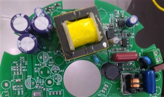
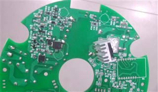
    Below are the images of Board for your reference:-


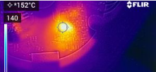
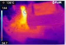
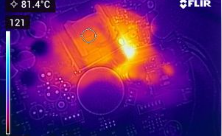
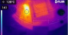
    Please also find herewith, the thermal images captured after 10 mins of running at 49.690W Load at  different hotspots:-

    Ambient Temp: 40C.

    1. Output Diode D3 (Temp: 83.8C)

    2. TVS Diode D2 ( temp. 152C)

    3. Resistance R6 (Temp. 136C)

    Although you had advised to remove R6, but after removing it & shorting its Pin 1 & 2, the efficiency of board dropped by 2%, so I connected it back.

    4. Transformer (Temp. 81.4C)

    5. Mosfet Q4(Temp. 128C)

    I had  earlier observed, the Temperature of Mosfet keeps rising, until it blows off, so I had to switch off the supply after 10 Mins.

    Please suggest, the improvements needed.

    Regards

    Subham

  • Hi Subham,

    I must apologize for the delay in my response. You're last post came in just before I took a two week winter break. It would seem that by now, your new board has arrived. Do you have new data and images to share?

    Regards,
    Ray

  • Hi Subham, it's been over a month since your last correspondence so I assume your issue has been resolved, so I will close this thread.

    If you need further assistance, please open a new E2E thread.