This thread has been locked.

If you have a related question, please click the "Ask a related question" button in the top right corner. The newly created question will be automatically linked to this question.

UCC28810: Power management forum

Part Number: UCC28810
Other Parts Discussed in Thread: TL431, PMP, TLV803

Sir, 

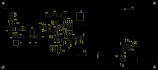
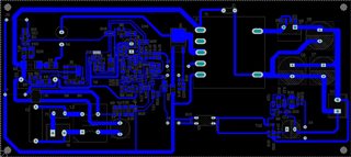
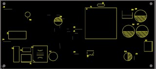
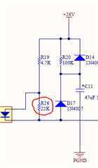
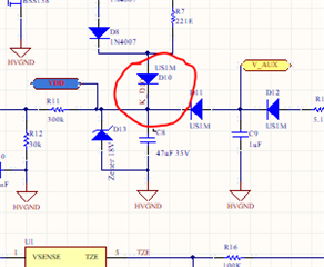
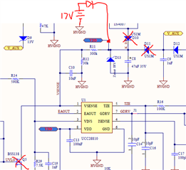
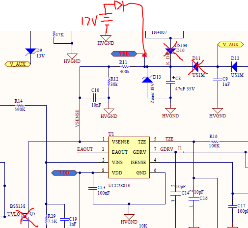
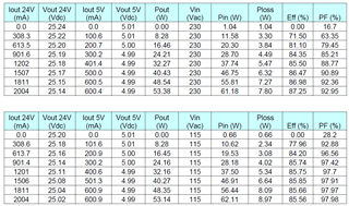
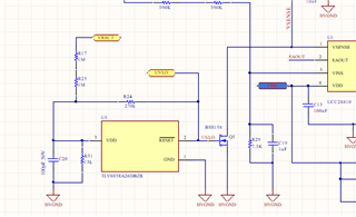
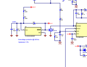
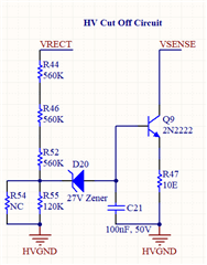
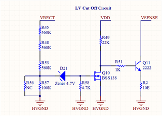
   Ref:, Design No. PMP30882,  We are designing 24V/2A Power Supply using TI's UCC28810 (LED lighting power controller). 

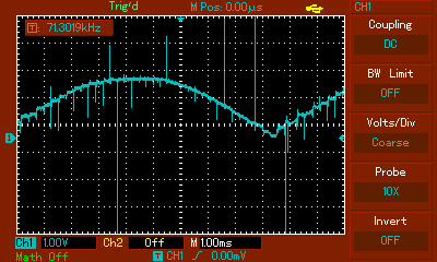
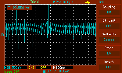
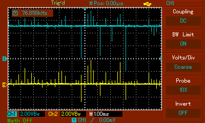
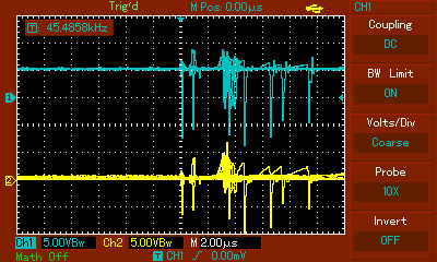
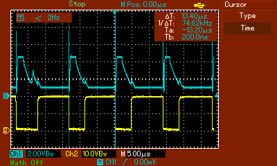
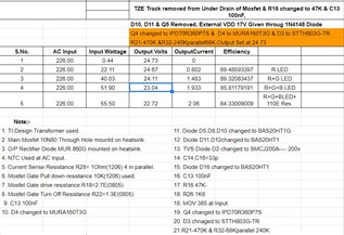
We were able to generate 24V regulated DC output at no load with Input range Vac 135V - 280V. 

We are facing the following issues, so need your support.

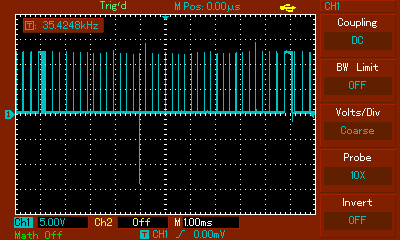
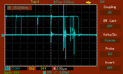
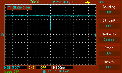
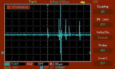
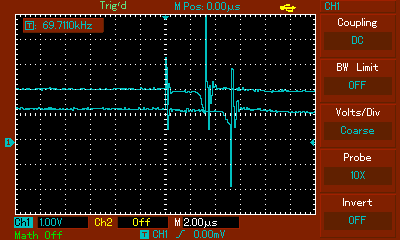
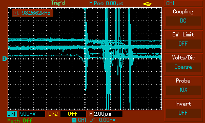
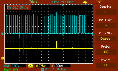
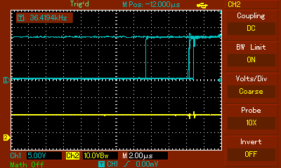
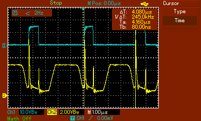
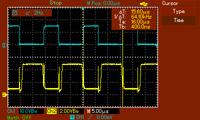
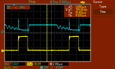
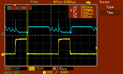
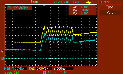
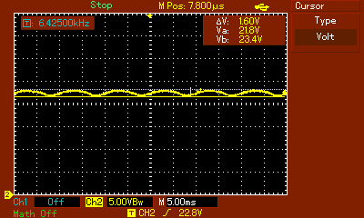
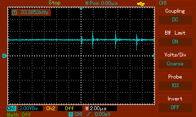
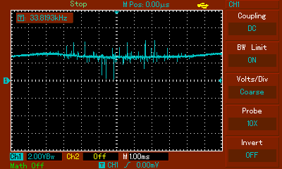
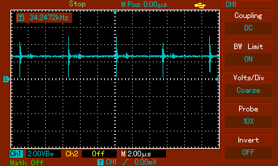
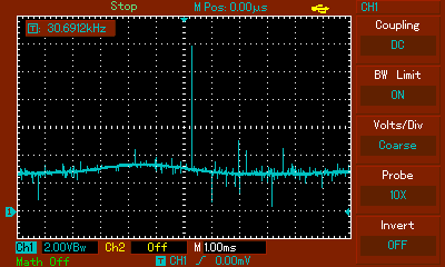
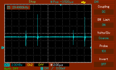
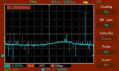
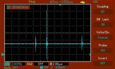
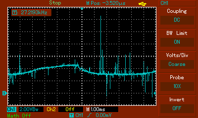
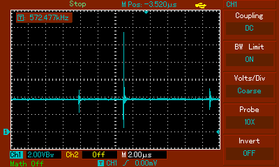
1. The output Voltage drops and starts fluctuating between 16 - 20Vdc even on 800mA load. 

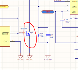
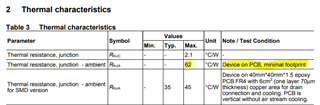
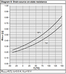
2. The Switching MOSFET(IPD70R360P7S) heats up a lot and blows off within a minute.

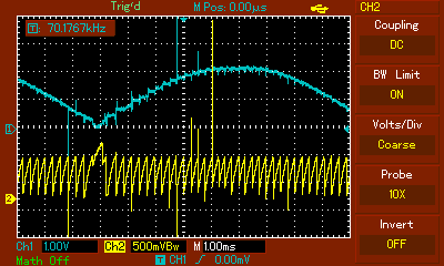
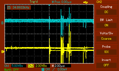
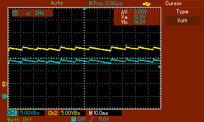
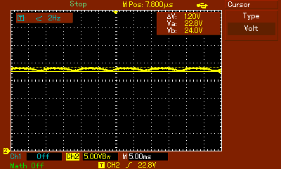
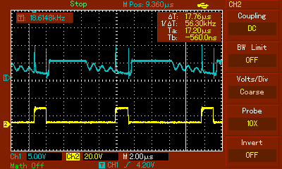
3. The Output Voltage appears at Input Voltage of 135Vac and not from 90Vac.

An early response would be highly appreciated. 

Thanks,

Subham

  • Hello Subham,

    I'm sorry to hear you're having trouble with your design.

    I cannot locate PMP30882 on TI.com. These are the reference designs for UCC28810: https://www.ti.com/product/UCC28810#reference-designs

    Perhaps this is an older reference design which is no longer on TI.com?  If so, can you please send me the files so I can see what you are using as a reference.

    Please also provide

    1. Your schematic (pdf is preferable)

    2. Your layout (.brd format is preferred if you can provide it)

    3. Waveforms of GDRV, VDD, VINS, VSENSE on a ~1mS/div scale, and on ~2uS/div scale when the output starts misbehaving. Please reference all signals to a major division to make it easy to read the voltages.

    Thank you,

    Ray

  • Hello Ray,


              Thank You for the response. Please find below, the schematic & layout along with the waveforms as required by you.

    1. Original TI Schematic(PDF Format)

    PMP30882 Rev_B Project (5).pdf

    2. Schematic of  our circuit.

    70W smps - Testing.pdf

    2. PCB Layout(.brd format)

    24V_Power Supply.brd

    3. GDRV Waveforms.

    3. VDD Waveforms

    4. VINS Waveforms

    5. VSENSE Waveforms

    If you require any more details or waveforms/test voltages, please let me know

    Waiting for your response.

    Thanks,

    Regards,

    Subham Kumar

  • Hi Subham,

    I'm sorry for the delay. I need a bit more time to study your schematic.

    A few things:

    • I can't open the brd file (viewer says it's corrupted). I'm hoping you can correct this so I can view the layout.


    • When I requested the waveforms, I was assuming you had a 4-channel o-scope. It looks like you're using a low-bandwidth probe with a digital meter. Do you have access to a 4-chan scope so that I can see the requested waveforms all taken at the same time? 
    • Is C8 right next to pin 8 of U1? If not, please put at least a 1uF cap right at pin 8 of U1 to pin 6 GND.
    • After you add the cap to VDD, please re-collect the waveforms with ~20mHz BW limiting (for now).

    Thank you,

    Ray

  • Hi Ray,

              Sorry for the BRD file issue. Please find herewith, the layout .brd format in correct version.(Please ignore the Airwire of HVGND, they are connected in PCB Through Jumpers and 0Ohm resistors)

    I checked the layout, Cap C8 is little far from pin 8 of U1, so I added a 1uF Cap right between pin 8 & pin 6 of U1.

    Sorry I don't have a 4 channel scope, so I am sending the waveforms on 2 channel scope with 20MhZ Bandwidth limiting.

    1. PCB Layout .brd format

    EXPORTED_PCB.brd

    2. GDRV & VDD waveforms.

    Ch1-GDRV

    Ch2-VDD

    3. VIN & VSENSE Waveforms.

    Ch1-VIN

    Ch2-VSENSE

    Hope this will help you in analysing the circuit.

    Please do let me know if anything else is needed.

    Thanks

    Regards

    Subham Kumar

  • Hello Ray,

           I also have another concern. The Efficiency of Power Supply is coming around 75%. I would like to have it around 90%. Please look into this also.

    Regards

    Subham Kumar

  • Hi Subham,

    Please provide transformer info.: Type, inductance, turns ratios.

    Thank you,

    Ray

  • Hello Ray,

    G084231LF ( EE-19 horizontal) This is the Transformer datasheet that we have implemented.

    Also can you please tell me the appropriate Voltages on Vins, Vsense and Isense pins of the UCC28810 IC according to the provided Schematic? This would be very helpfull. 

    Thank you,

    Subham Kumar

  • Hi Subham,

    I'm having a little trouble reconciling the transformer in your design with the pinout of the G084231LF. I would expect it to look exactly like the transformer in the reference design. Perhaps you have a datasheet you can share?

    I'm also curious why you didn't utilize the TL431 in your feedback loop.

    VINS is simply the rectified line voltage divided down by R9, R11, R14. It would equal Vinac/sgrt(2) x 7.32/1187.32

    VSENSE is VDD divided down by R6, R8. So VDD x 30.1/331.1

    ISENSE is your switching current x R15

    I still can't open the .brd file. Can you just take a screen shot of each layer save as .jpg or similar for now.

    Please also provide the EAOUT with +24V, and ISENSE with +24V

  • Hello Ray,

    Thanks for the prompt response.

    Please find below the Design Details of Transformer used in the Power Supply.

    Transformer TI forum.pdf

    We have updated the feedback loop with TL431 circuit and still facing the same problem of voltage drop on Load.

    Please find below, the JPG image of Bottom Layer, Bottom Overlay, Top Overlay & Bottom Solder Layers of the PCB.

    I have checked the EAOUT & ISENSE Voltages on Load.(Output Voltage had dropped to 18.18V on 24V/800mA LED Load)

    Vac=230V

    Iout=250mA

    EAOUT=4.98V

    ISENSE=12mV

    Also find below the observed waveforms for EAOUT & ISENSE.

    Thanks

    Regards

    Subham Kumar

  • Hi Subham,

    After closer inspection of your schematic, three major issues were identified:

    1) D2: You're using a 100V Zener here. The 100V is causing Q4 to work very hard to try to regulate the the primary and this is likely why it is burning up. This needs to be at least 1.5x your primary voltage (4 x 24.5V) which is why the 150V device was chosen for the reference design. 200V would be better and still provided protection on Q4.

    2) The Feedback loop: Now that you've used the TL431 feedback loop, please use the resistor values similar to the reference design for R21 and R24 (your R21, R32). I used the term "TL431" generically, so if you used a non-A version, you should change your R22 to ~510Ω to provide enough bias current. However, if you used the ATL431 as is used in the reference design, you can leave R22 as it is.

    3) D9 is an 18V Zener. This should be 13V like the reference design. It is likely keeping the current source on all the time which is drawing power, reducing your efficiency.

    Let me know how things work after you address these.

    Ray

  • Hello Ray,

                We made the changes as suggested by you.

    1. Now for D2, we are using 2 Nos 100V Zener in series to make up for 200V.

    2. In our Feedback Circuit, we are using, KA431AZ, so changed the biasing resistance to 510 Ohm.

    3. D9 is now 18V.

    After making all these changes, I checked the circuit. But still the voltage is dropping on Load as earlier.

    Following are voltages noted on UCC28810D Pins after above changes:-

                                                                           No Load                     On Load(24V/800mA LED Load)

    Vout                                                                     25.37V                                            17.5V

    Vaux                                                                         13V                                           12.48V

    VDD                                                                       13.3V                                           12.04V

    Vsense                                                                    1.2V                                           370mV    

    Vins                                                                       1.35V                                               1.2V

    Isense                                                                         0                                               63mV

    Iout                                                                                                                             250mA

    After this, I changed R12 (Potential Divider resistance at VSENSE PIN) to 51K from 30K. Its R8 in TI schematic.

    Now the Voltage at Vsense Pin at No Load rose to 1.9V, & on Load it was almost same 300mV.

    But interestingly, my Output Voltage on Load was now  18.8V.

    Followed by increasing voltage at Vins by changing R29 to 12K. from 7,5K. Its R14 in TI schematic.

    Now Vins voltage was 2.3V.

    And on same Load, Output started gradually increasing upto 22V, but I had to Switch OFF the circuit as my main Mosfet Q4(Q1 in TI schematic) became very hot.

    Thanks

    Regards

    Subham Kumar

  • Hi Subham,

    I suspect there's still something wrong with your feedback loop (or a part has been mis-populated somewhere on the board) as you should have seen a big improvement.

    Can you send a schematic with the updated connections?

    The issue may be that I mistakenly gave you the RefDes from the ref design (R22). I meant to say that you need to change your R26 to 510Ω. If you didn't change this, it will explain why your loop still isn't working. The KA431AZ looks like it needs >1mA.

  • Hello Ray,

             Please find below, the updated schematic, currently being used by us for  Testing.

    2577.70W smps - Testing.pdf 

    We are still facing the problem of Voltage Drop on load even after changing R26 to 510 Ohms.

    Also the MOSFET IPD70R360P7S is getting too hot to touch on Load.

    Regards,

    Subham

  • Subham,

    The updated schematic you shared still shows R26 = 22kΩ. For now, I will assume you've changed that and you've made all of the changes suggested above.

    At this point, the schematic should be essentially identical to PMP30882 so it should regulate.  At this point, I can only think of two areas that may be causing the issue:

    1) Layout. I really can't make out much from the layout picture's you've provided (resolution is too low). From what I can see, there doesn't seem to be any consideration made for ground shapes and many of the lines are long and narrow. Did you follow the layout from PMP30882?

    2) A build issue:

    • Perhaps one or more components on your board don't match the schematic
    • There may be a short or open somewhere that is unexpected
    • Solder flux on the board causing resistive shorts between nodes

    If you get the same results on another board, we can eliminate those last two bullets. However, the first one would still be a possibility

    1. If you haven't already, please modify a second board as you have this one and see if it behaves the same
    2. If two boards behave the same, please verify that the component values match the schematic.
    3. Once you've confirmed the board matches the schematic, please recollect the waveforms. However, the resolution that you provided in the past are too low of bandwidth and so they aren't helpful. See if you can get a better oscilloscope with higher bandwidth and sample rate.
    4. Try to generate .brd files that I can open them with Cadence Allegro.

    Thank you,

    Ray

  • Hello Ray,

    Thank you for the feedback. I mounted the components on different PCB with slightly improved Layout and I am now getting 40W output.

    There are still some problems that need to be fixed.

    1> The MOSFET IPD70R360P7S getting Untouchable hot very quick even on 1.0A Load. 

    2> After increasing load to 1.5A it blows off in a minute or two along with the Current sense Resistor(2X 0.470E in Parallel) connected in series with its Source.

    3> I am also getting around 86% efficiency which is quite low as per the expectation.

    Please suggest some modifications which can be incorporated in the circuit to achieve the expected output.

    Thank you,

    Subham

  • Hi Subham,

    Glad to hear there has been improvement.

    You need to manage the power through Q4. Just looking at your board, you don't have much metal area available to pull heat out of the MOSFET. You should probably attach a heatsink to the body of Q4 to help dissipate the heat.

    Make sure your sense resistor is properly sized for the power (over design it for now until you get to the root cause). The resistance will go up with temperature and if it gets too hot, the resistor will be damaged and the resistance will be changed permanently, even after it returns to room temp. 

    Make sure you're using an isolated input source, or your scope grounds may be creating an unintended ground path.

    There's not much more I can help you with, especially without quality scope shots.

    Your schematic looks reasonable and if you've confirmed the component values on the board, this may be related to layout. Here's an EVM with a similar design. Refer to fig 2: https://www.ti.com/lit/ug/sluu344b/sluu344b.pdf

    This color overlay of the top and bottom layer may make it easier to see:

    Ray

  • Hello Ray,

           Thanks for your consistent support & feedback. Now I have been able to achieve 24V/60W from the power supply with little improved layout.

    The main issue now being faced by me is that, although SMPS works fine with or without Load, but sometimes while switching ON/OFF the AC Input to SMPS, the Main Mosfet Q4(TI schematic) blows off. 

    Should I use Schottky Diode BYS10-25-E3/TR at Gate of Mosfet, as shown by D16 in https://www.ti.com/lit/ug/sluu344b/sluu344b.pdf ?

    Or Please suggest, what you think could be the reason.

    Plus I am still not satisfied with the heating issue of Mosfet Q1 & Output Diode Rectifier D6. (As per TI Schematic).

    1. I am using Mosfet STP6N80K5 in place of  IPD70R360P7S(in TI schematic). It gets heated a lot on load, though i assume the current through it must be very much less than its rating. So now I am planning to use the STF10N80K5, TO 220 Package mounted on heatsink.

    2. For Output Diode Rectifier, I am using MUR 860G, in place of STTH803D(in TI schematic.). It also was getting quite hot, so I mounted it on heatsink, but still the case Temp is going around 100  C.

    Should I use R1 & C3(Snubber across D3 in TI Schematic)?. They are shown as DNP. So please suggest the values of Resistance & capacitor to be used.

    Thanks

    Regards

    Subham

  • Subham,

    Your schematics always indicated you were using IPD70R360P7S and STTH803D. However, all this time you've been using a different MOSFET and rectifying diode than what was indicated in the schematics you provided. It's important to share accurate information about your design so that I can more effectively help you. Yes, the heatsink on Q4 will help a lot.

    You should only use the snubber if you're getting ringing across the diode. A snubber will reduce your efficiency. According to the schematic, R4 is ERJ-8RQFR22V and C4 is GRM21BR6YA106KE43.

    Regards,

    Ray

  • Hello Ray,

                  Really Sorry for the the inaccurate  information in the schematic. I hope you will not mind & continue your invaluable support.

    Now i am attaching the updating schematic, with the complete information of Mosfet &  Rectifier Diode being useed.

    I have used a NTC at Input Ac supply of SMPS as my Mosfet was blowing Off on On/Off switching of AC supply. NTC had helped me sort out that problem a lot. Plus I have also changed the Resistance Values at Gate of Mosfet  R22 & R18(Current schematic) for fast Turn OFF. Please check.

    3175.70W smps - Testing.pdf

    Now I have been  successful in drawing a output Load of 35W from the supply.

    But there are some issues that remain to be resolved.

    1. On increasing output Load to 2.0 Amps, (48W), the Mosfet Q4 & Diode D3(Current schematic) start heating up a lot.

    Within 5 minutes the Temperature of Mosfet raised to  88C & Diode to 82C. And with that the Mosfet Q4, R28, R18,R22, D1,D13(current schematic) blew Off. i tried this 2-3 times, with same result every time. However in 1 case the main IC UCC28810 also blew Off.

    2. With 48WLoad connected at output, on switching On/Off the AC Input, the same problem was encountered. However supply works fine with 35W Load at output.

    3 Currently the efficiency of supply is around 88%, i would like to have it above 90%.

    Please suggest the modifications & improvements required  in circuit.

    Thanks

    Regards

    Subham

  • Hi Subham,

    Thank you for updating the schematic to accurately reflect your design. It is my pleasure to support you; having accurate information helps us both to try to find a solution to this issue.

    Can you confirm that D13 and D1 are damaged? If so, please tell me the part numbers you are using.

    Just for debug, I suggest disconnect some non-critical functions from the controller:

    • Disconnect the UVLO circuit by removing Q5. Make sure everything still works as before.
    • Then remove D10 to disconnect the quick startup network. Check again that everything still works.

    If it all still operates, try again at 48W and see if there is an improvement.

    Also:

    Would it be possible for you to borrow a better oscilloscope to get meaningful waveforms?

    A current probe so we can see the transformer currents?

    Regards,

    Ray

  • Hello Ray,

           Thanks for the feedback.

    As per my current schematic, D1 is ABS210 & D13 is BZT52C18.

    Every time Mosfet Blows off, they also are damaged & I have to replace them.

    I made changes in circuit as per your suggestion:-

    1. First I removed Q5. The circuit worked as before with no improvement.

    2. Secondly I removed D10, but this time, the circuit gave no Output.

    I also checked by removing D10, as per TI schematic, but still there was no Output.

    Now I have also, incorporated a gate pull down Resistor R43 in circuit. Below is the schematic.

    4300.70W smps - Testing.pdf

    I also tested the Power supply on 1.2 A Inductive Load. After 40mins, following temperature was observed on the components:-

    Mosfet Q4- 85C

    Rectifier Diode D3- 75C

    Transformer T1- 59C

    (Ambient Temp 28C)

    Efficiency was 86%.

    1. I have to use the Power Supply to draw a current of 2.5A (60W)

    2. Efficiency to be > 90%.

    Please suggest modifications/changes required in circuit.

    Regards

    Subham

  • Hi Subham,

    I apologize, but I forgot to tell you that you need to connect a supply to VDD when the startup circuit is removed. Please also remove the Aux from that node so to focus only on the regulation of the output. Use a diode to isolate the supply. See below:

    Ray

  • Hello Ray,

    I made changes in circuit as advised by you. Present ally I am testing the circuit on LED Load, but my requirement is of 2.5Amps Inductive Load.

    Following are the observations after modifications(D10,D11 & Q5 removed

    1. The circuit worked fine on Output LED Load of 17W, efficiency was 87%. 

    Temperature readings were as below:-

    Mosfet Q4- 44C

    Diode D3- 63C

    Transformet T1-47C

    2. When I switched On the circuit on 33W LED Load connected, within 1-2 Seconds, it blew Off.

    Main Mosfet Q4, IC UCC28810,Current Sense resistance R28, Gate resistances R18 & R22 were damaged.

    Please suggest

    Regards

    Subham

  • Hi Subham,

    The designer of PMP30882 has been tied in in a separate email thread. I will follow up with you when he provides his input. I'm hoping to give you a response today, but please allow up to a few days so he has a chance to go through everything we've already discussed.

    Regards,

    Ray

  • Hi Subham, I don't know if you received the email response from the PMP30882 designer. I'm pasting it below:

    1. Schematic:
      1. Diode D18: I see here a 1N4007 is used. This is a standard recovery diode (and very slow), so I am not sure it should be used here. I suggest to replace it with a 1N4148, who has few nanoseconds trr
      2. Diode D3: tin my design I opted for a 300V diode, where we have here a 600V rated. This traduces into increasing conduction loss and higher temperature. Please provide enough cooling here (I see the customer is already using a heatsink for it).
      3. MOSFET Q13: the switching characteristics are pretty good, but the Rds(on) is double compared to my original design; that means the efficiency will suffer and temperature will increase; so, use an heatsink also here
      4. Transformer: from the datasheet of this transformer, I see that the specs are correct in terms of inductance and turns ratio.  I didn’t understand if all dots are correctly place: I mean, the specs says the secondary side stars on pin 6 and it’s wound clockwise….please double check it. A simple way to check whether the secondary side is correctly connected is to watch the switch node (pin 3 of TX1) on primary side (with an isolated HV probe) and pin 10. When the MOSFET Q13 is turned on, the voltage on pin 3 should go to zero, while the voltage on pin 10 should go negative. Please double check also this.
      5. I see that the transformer is correctly developed, with the dot on primary side (pin 1) starting with the first turns and placed in the inner layer. This is done in order to shield the first turns of the winding, which are switching at high dV/dT, compared to secondary winding. The point is that the switch node Q13 drain should be connected to pin 1 and not to pin 3. The advantage of swapping pin 1 and 3 of TX1 (and at the same time swapping pin 4 with 5 and pin 10 with pin 6) is that there will be less noise in the EMI measurement. I understand that swapping all pins makes a “mess” in the board, but the customer might consider in case there is a board layout re-route. Anyway, I don’t think this is the reason for the failures.
    2. Board layout: I believe it can be improved, but should not be the cause of failure. Anyway, I suggest , in case of a revision, to improve it as follows:
      1. Avoid placing components beneath the drain of Q13: here we have high dV/dT
      2. Remove the net of pin 5 of U1 (TZE net): this net is sensitive and it is routed beneath the drain of Q13
      3. I see some ground return (like R28) coming back to ground pin of C4 with pretty long track: this should be minimized.
      4. Also the connection from ground of R28 and ground of U1 should be minimized to avoid noise in the current sense signal (pin 4 of U1, ISENSE).

    Now some thoughts about the possible reasons of failure:

    • At first sight I thought that there was high inrush current during switching on, but the customer tested also a version with an external 10 Ohm NTC, so it should be excluded.
    • Then, if the dot on pin 10 or 6 of TX1 is wrong, it might explain why the MOSFET blows up, because it tries to charge C6, C6 and C7 in almost zero time, yielding a huge inrush current….but having a wrong dot on the secondary side of the transformer would make the converter working really bad!
    • Since I have done in the past lot of similar designs, and nobody experienced any failure, I think we should consider the AC source and its impedance: are they using a variable transformer? If so, what is the nominal power of this transformer? I am asking because a low power variable transformer might have pretty high inductance, which at startup might resonate with C4, producing high low-frequency ringing on this capacitor (maybe reaching kV and destroying Q13). In any case, I suggest to add a 275VAC varistor in parallel to C2, and check if it solves the issue. If not, please check with the oscilloscope, during startup and using low AC input voltage (to avoid destroying the converter each time it’s switched on) and check if there is any overvoltage on C4.
  • Hello Ray,

            Thanks very much for the suggestions & feedback provided by you.

    I am incorporating the changes & modifications  as advised by you in the circuit and shall get back to you soon.

    I was checking the Voltages & waveforms at each pin of UCC28810 & while going through the  Leading Edge Blanking circuit in datasheet of UCC28810. 

    I have changed C18 & C19(C14 & C16 in our circuit) to 44pF(nearest value available to 47uF) and R27(R16 in our circuit) to 22K as per datasheet.

    Following waveforms were observed at Gate & TZE pins of UCC28810. I see a Overshoot at TZE pin at the time of  Gate Switching, more prominent at Gate switch  ON. .

    Ch1-Gate

    Ch2- TZE Pin

    600mA Load

    Ch1-Gate

    Ch2- TZE PIn

    1.2A Load

    Regards

    Subham

  • Hello Ray,

          I am also sharing the waveforms observed on TZE Pin & GDRV Pin on Circuit as per the original TI schematic for comparison. No components were changed in this circuit. Please find herewith the schematic again for your ready reference

    6428.70W smps - Testing.pdf.

    Below are the waveforms:-

    Channel 1--- TZE

    Channel---   GDRV

    Load--- 600mA


    Above 2 waveforms observed on same load at different time interval. As  can be seen, gate pulse period is different in both, consequently switching frequency is 106KHz & 72Khz respectively.

    Please also check below the waveforms at 1.2Amps Load.

    Channel 1--- TZE

    Channel---   GDRV

    Load--- 1.2A

    In above waveforms Frequency observed was 89 & 72KHz respectively. Consequently duty cycle is 29% & 64%.

    Is this much variation in Frequency & Duty Cycle normal?

    Regards

    Subham

  • Hello Ray,

                 Today I have also captured the VDD waveforms at No Load Start Up, Running at No load.

    As it can bee seen, at start up the voltage goes switches from 16.2V max to 10.0V min for some cycles before it settles at about 13V (shown in next picture) Is it normal ?

    When supply is running at No Load, following waveform was observed.(Varying from 15V to 13V), as can be seen below:-

    It is normal to have such peak to peak difference of about 2V ?

    Further on increasing the load, the VDD increases upto 18.6 V

    1. No load -> average VDD 14.0V

    2. ~700mA load -> average VDD 16..5V

    3. ~1400mA load -> average VDD  17.5 V

    4/ ~2000mA load -> average VDD 18.6 V

    Is this normal to have VDD increase that high ?

  • Hello Ray,

            Could you please also share your Sample Layout for UCC28810 power supply, so we can compare & take Inputs from it for reference.

    Regards

    Subham

  • Hello Ray,

       I also observed the Vdc Output waveforms at different  Loads & following are the waveforms:-

    Output is fluctuating/ringing. Please specify what could be the reasons:-

    740mA Load

    1.2A Load

    2.0 A Load

    Regards

    Subham

  • Hi Subham,

    1. Regarding VDD, it appears to be cycling between regulation and UVLO. Early on I had asked you to add a cap on VDD which you did. However, I don't see it in the schematic you just provided.

    The controller may be being starved for bias current resulting in VDD dropping under UVLO, a larger cap right at the pin will help if that's what is going on.

    Also, the intention was to remove the VDD startup and UVLO circuitry as is shown below until we get past the output regulation issue. Removing this circuitry and supplying VDD externally as well as adding a cap from pin 4 to pin 8 (right on the device) should keep VDD steady.

    2. Please respond to the PMP designer's questions 1d & 1e from 5 days ago. Include the waveforms he requested. I've repeated them here:

    ...the switch node (pin 3 of TX1) on primary side (with an isolated HV probe) and pin 10. When the MOSFET Q13 is turned on, the voltage on pin 3 should go to zero, while the voltage on pin 10 should go negative.

    3. Attached are the artwork files from the UCC28810 EVM:

    HPA483B.PCB

    Please address 1 and 2 above so we can help you to isolate your core issue.

    Thank you,

    Ray

  • Hello Ray, 

               Please find below my observations on the PMP Designer's feedback:-

    1. Schematic

    a. I am already using the Diode 1N4148 for D18.

    b. & c- I have Ordered the same Diode D3 & Mosfet Q13, as per your design & shall modify as soon I receive them. In the meantime I am checking the other parameters of Power Supply.

    d. I checked the Transformer. The secondary side starts from Pin 6 & is wound clockwise. Plus I also checked the waveform On Node 3 & 10 of Transformer as advised by you. When Mosfet Q4 turns On, the voltage on Pin 3 goes to zero, while the voltage on Pin 10 goes negative,

    e. In TI schematic, the Transformer Primary Start Node is connected to drain of Mosfet And start node of Auxiliary winding is connected to 5.11E Res for         V auxiliary while start node of secondary winding is connected to diode D3. However in our layout, Pins 1&3, 4&5 and 6 &10 have been swapped altogether as compared to original TI schematic.

    I checked all the waveforms at Transformer Nodes even by swapping all the pins to make it look like as TI original schematic, but same waveforms were observed as earlier. So iI don't think that could be the issue.

    Finally as you suggested, if Pin 6 & 10 of transformer are interchanged it might lead to blowing OFF of Mosfet due to huge inrush charging current of capacitors. So to recheck my Pin 6 & 10 orientation I tried  by interchanging Pins 6 & 10 on No Load, but that immediately leads to increase in Input wattage. So I can say my Pins 6 & 10 have been connected correctly.

    Now I have few queries about the waveforms observed at different Pins, which I would like you to clarify:-

    1. Following waveforms were observed at Gate & TZE pins of UCC28810

    Ch1-Gate

    Ch2- TZE Pin

    Load 740mA

    Above 2 waveforms observed on same load at different time interval. As  can be seen, gate pulse period is different in both, consequently switching frequency is 106KHz & 72Khz respective

    Please also check below the waveforms at 1.2Amps Load.

    Channel 1--- TZE

    Channel2---   GDRV

    Load--- 1.2A

    In above waveforms Frequency observed was 89 & 72KHz respectively. Consequently duty cycle is 29% & 64%.

    Is this much variation in Frequency & Duty Cycle normal?

    Plus I see a Overshoot at TZE pin at the time of  Gate Switching, more prominent at Gate switch  ON also, how to control it?

    Regards

    Subham

  • Hi Subham,

    Thank you for verifying the inductor pinout. I will consult with PMP designer.

    In the meantime, please comment on #1 in my previous response regarding VDD as well as the designer's question on the A/C source.

    Regards,

    Ray

  • Hi Subham,

    With a constant current, the off-time and frequency will vary along the rectified input waveform, so that is normal. However, the on-time should be constant regardless of where along the input cycle it's measured. It's not constant.

    his may be because the controller is running in DCM at this load. From your ZTE signal, it appears that this may be the case. This can also be observed by monitoring the drain voltage of the MOSFET. Resonant ringing would be present if it's operating in DCM. To correct this, reduce R16 (down to 68kΩ or even 47kΩ) and see if this corrects.

    Another possibility is noise on the EAOUT pin. Make sure C18 is close to that pin (U1, pin 2).

    Ray

  • Hello Ray,

                  We removed D10, D11 & Q5 as advised by you & gave External VDD 17V Supply thorough a Diode. The TZE path that was going beneath the drain has been cut and a wire was connected resistor value was also changed from 100k to 47k as per your feedback. And following are our Observations.

    1. No sign of ringing at the TZE pin. So I guess it is now not operating in DCM mode anymore.

    2. The SMPS working fine till 35W output load(LED strip light), we are getting 87-89 % efficiency. But as soon we increase the output load to 45W, the input wattage seen rushing exponentially(we reduced load when it reached >60W) immediately, while the Output wattage remains near constant.  Could you please tell us what could be the reason to this?

    3. The same result 2 is reflected on 35W load when DSO is connected.

    Your feedback is appreciated kindly suggest the potential solution to this. We will be looking forward to hear from you soon.

    Regards,

    Subham

  • Hello Ray,

               We have made following changes in the Design and now the SMPS performance has improved a little.

        1. Switching MOSFET Changed to IPD70R360P7S(as per TI)

        2. Output DIODE changed to STTH803 SMD(as per TI)

        3. Snubber Diode D4 changed to MUR160G(As per TI) from US1M

    We have tested the SMPS on 47W LED Load with external VDD and with Internal VDD both. TL431 reference Voltage resistors also changed (R21 = 470k) and (R32 = 68k || 240k) to get 24.7V  output.

    1. Below are our observation with external VDD of 17V as you suggested earlier:-

    2a. Below are our  observations with Internal VDD.

    2b. Below given the thermal report with internal VDD at 1.4A load 

    2c. At 47W load the Body Temperature of MOSFET seen rushing to 93 deg Cel. within 1 Minute of operation and we had to reduce the load for precaution. Can you please tell us what is the acceptable body temperature of MOSFET running at 2A Load? 

    Also How can we increase the OUTPUT regulation further as it is below our expectation?

    The updated schematic has been attached herewith for your reference. The changes that we have made in the schematics are also reflected in the given reports.

    24 V Power supply (1).pdf

    Thank you,

    Subham

  • Hi Subham,

    For 2A load @ 24V ~ 50W, it would not be unreasonable to have ~1W dissipated in the MOSFET. From the datasheet, this would result in ~62°C rise above ambient. So 62°C + 25°C is 87°C which is about where you are. At 1.5W, which isn't unreasonable, you'd be at 118°C.

    As the temperature rises, the RDSon of the MOSFET also rises. This in turn generates even more loss, resulting in more temp rise, etc, etc. This is where you can get into a runaway thermal loop. Sufficient heatsinking is CRITICAL.

    1. Other components (like the transformer, diode, bridge, thermistor) will also dissipate heat. Use a thermal camera to capture the heat measurements of the entire board at your different load conditions. This will provide valuable information as to which components are heating up and by how much. Please share.

    2. Please provide a photograph of your board so I can see how components are heatsinked.

    3. I recall you had changed your board layout. Can you share that file? Altium is preferable but images will be ok.

    4. With minimum Vin, at what power does the temperature start to run away? 

    5. Before the excessive heating occurs, your efficiency numbers are close to the expected (actually better). These are the numbers from a similar design. At 230Vin, 24Vout, 1.5A, efficiency is 86.5%. You're at 88.6%.

    Regards,

    Ray

  • Hello Ray,

       Thank you very much for your valuable feedback. I shall share the data as requested by you.

    In the meantime I would like your suggestion on few more points:-

    1. In the BOM of Power Supply, I have cost considerations involved. So I am unable to use TLV803EA26DBZR for High Voltage Cut Off. Could you please suggest any other cost saving component/circuit for High Voltage Cut off.

    2. Secondly , I also have to incorporate Input Low  Voltage Cut Off in the power Supply circuit. So please also suggest circuit for the same.

     Regards

    Subham

  • Hi Subham,

    The TLV803EA26DBZR is not in the schematic for high voltage cutoff. It provides low voltage cutoff as you desire. Is this clear?

    Also, it is $0.145 in 1000 pc qty. I'm not sure that the additional components that substitute circuitry may require will be less than that. At least not by much. 

    If you want to eliminate some cost and you can tolerate a slow turn on (~10 sec), D9, R8, R9, Q3, D5, D8, Q1, R7 could be eliminated.

    Ray

  • Hello Ray,

             Thank you very much for your feedback.

    This is in reference to the circuit of TLV803EA26DBZR.

    Please consider the schematic section below:-

    From my understanding of circuit, TLV803EA26DBZR gives a reset signal to VSense pin of UCC28810 whenever voltage exceeds its limit.

    From the datasheet, I can see that   TLV803EA26DBZR is a Voltage supervisor IC with  Active Low Output & threshold voltage of 2.64 V.

    So from my understanding, whenever voltage at VDD pin of TLV803EA26DBZR goes below 2.64 V , it shall send a low signal at its output, t to gate of Q5. In normal circumstances, I have observed, voltage at its VDD pin remains lower than 2.64, so it sends a low signal which keeps the Mosfet Q5 Off & lets UCC28810 work as per its VSENSE voltage etc.

    At High Input Voltage, Voltage at its VDD pin goes above 2.64V & at that time it sends a High signal(Its default state) & that Turns On the Q5 Mosfet & thus VSENSE of UCC28810 is pulled low than Enable state & this stops Gate Signal to Main Mosfet Q4, turning it OFF. So I assume, TLV803EA26DBZR is being used for High Voltage Cut Off.

    Also consider the schematic shared by TI.( PMP30882)

    Below the circuit for TLV803EA26DBZR, its mentioned Overvoltage Protection @303Vac.

    Please clarify the functionality of TLV803EA26DBZR.

    And if its for High Voltage Protection, then request you to share relevant circuit for Low Voltage Cut off.

    But conversely  if it provides Low Voltage protection, then please share the relevant High Voltage Cut Of circuit for the same.

    Waiting for your valuable suggestions & feedback.

    Regards

    Nitin Gupta

  • Hello Subham, Nitin,

    You are correct, That is set up for OVER voltage detection (I was mistakenly looking at a different version of the supervisor IC).

    It you want to add under voltage detection, you should look into a dual channel (or window) supervisor IC rather than the TLV803EA26DBZR. See the list here: https://www.ti.com/power-management/supervisor-reset-ic/products.html#p1455=2;2

    Looking forward to you responses to our earlier correspondence.

    Ray

  • Hello Ray,

                Thank you for your response.

    I need your support for the below High Voltage & Low Voltage Cut Off circuits.

    Please find below herewith, transistor based  Over Voltage & Under Voltage Cut Off circuits. 

    Kindly suggest if these circuits can be incorporated in the UCC28810 Power supply circuit, or need any modifications.

    Over Voltage Cut Off

    Low Voltage Cut Off

    Looking forward to your valuable feedback

    Regards

    Nitin Gupta

  • Hi Nitin,

    Regarding the LV cut off circuit, when VRECT is < 83.7V (59Vac), Q10 will be off and Q11 will conduct pulling VSENSE low (which is what you want). Be aware that you will always be burning power through R45/R48/R53/R57/D21/R58 and when VRECT is > 83.7V (59Vac), Q10 will be conducting and will burn ~13mW through R49.

    For the high voltage cut off which activates at 405V (286Vac), I don't see a connection to the UVLO node.

    This may not be a concern of yours, but please be aware that neither circuit has hysteresis to prevent chattering near the thresholds.

    The benefit of the supervisor IC is that it is powered by and monitors VDD (and many have programmable hysteresis). I would strongly suggest you consider one of these ICs (which are relatively inexpensive). Looking at their datasheets, you won't need as much external circuitry. If you do chose to use a dual-input supervisor, please open a separate E2E thread. This will allow a supervisor IC product expert help you to make sure you've chosen the best part for this situation and advise you on the design.

    Regards,

    Ray

  • Hello Ray,

    I would like to ask some doubt regarding the SMPS.

    1A. What  components do I  need to change if I want to change the Switching MOSFET? Please advise.

    1B.  Should I consider other MOSFET's rise time, fall time, input capacitance and gate charge etc, in that case other than Rdson, Vgs, Vds?

    1C. What is the recommended procedure for selecting proper Mosfet in SMPS & associated Components viz, gate resistance etc.  for  proper operation?

    2. Also I would like to use TLV803EA26DBZR as Under Voltage protection as well. This makes 1 TLV803 for Overvoltage protection and 1 for Undervoltage Protection. Please review the circuit as below for Low Voltage Cut off:-

    Thank you,

    Subham

  • Hello Ray,

               In continuation with my query regarding the Switching Mosfet above, I need your support on improving the Regulation & Efficiency of Power Supply.

    I have designed a new Board for it. Please find below the schematic & PCB Layout File :-

    24V SMPS V2.zip

    I tested this board on Load & following is the Regulation & Efficiency observed:-

    1. As you can see from above Table, at 800mA, the efficiency is around 89%, but starts dropping after that. At 2 Amps, its only 84% & drops more after that.

    Please advise how to correct it. I wish to have Efficiency around 88-90%.

    2. Also, as you can observe regulation is very poor after increasing load more than 800mA. 

    I need you support to improve Regulation & Efficiency of my Board.

    Thank You

    Regards

    Subham

  • Hi Subham,

    Please provide the information requested several weeks ago as that will allow me to help you to try to locate areas where you may be experiencing power loss:

    1. Other components (like the transformer, diode, bridge, thermistor) will also dissipate heat. Use a thermal camera to capture the heat measurements of the entire board at your different load conditions. This will provide valuable information as to which components are heating up and by how much. Please share.

    2. Please provide a photograph of your board so I can see how components are heatsinked.

    In the meantime, I will look over the information you provided.

    Regards,

    Ray

  • Hello Ray,

     I observed the SMPS circuit at Minimum Vin as advised by you. My Minimum Vin requirement is 120V.

     Input set at 120V & Output Volts 24.26 V

    1. At Output Load of 1.5A circuit worked fine.

    Vout= 24.21V 

    Pout= 36W

    2. At output Load of 2A, O/p Volts dropped to 23.25

    Pout=46W

    And also the Temperature of Mosfet started increasing very rapidally.

    I wish to draw 2.5A at 24V with improved regulation & efficiency at Vinput =120V.

    Please suggest.

    Also kindly suggest, the various parameters required to be taken into consideration along with suggested values & calculations if any Viz: Input/Output capacitance, Rise, Fall Time etc for main Mosfet along with associated components like Gate Turn On/Off resistance etc. as asked by you in earlier post. 

    Regards

    Subham

  • Hello Subham,

    To improve your efficiency, it is important to identify areas of power loss on your board. The purpose of providing a thermal image was to identify components other than the boost FET which are impacting your efficiency. As we discussed before, the heating of the MOSFET is normal (62.5°C/W) which in turn will negatively affect efficiency. To that end, you were going to add heat-sinking to the boost FET and diode. I don't see either on the Altium file you shared.

    How hot is the output rectifying diode D3 getting? The transformer? The bridge?

    D3 is likely burning power during recovery. Consider changing to a SiC diode to reduce reverse recovery loss in that component.

    I'm curious why the output is dropping. Can you measure EAOUT for each power level (especially just before the output drops, then a bit after and then at full load)? I'm wondering if the feedback loop is being saturated.

    Afterwards, it may be worthwhile reducing your current sense resistance by ~10% to see if that has an effect on the output (in case current limit protection is kicking in).

    Ray

  • Hello Ray,

    A) I noted  the Temperature Readings on Output Rectifier Diode D3, Transformer T1 & the Bridge D1. Following are the observations:-

    S.no.  Time I/P AC O/P Volts Load Mosfet Q4 Diode D3 Transformer T1 Bridge D1
    1 To    220 V    24.23 V 0 23.6 C 24.6 C 24.6 C 24.5 C
    2 To+10Mins    220 V    23.8 2.11 A 100 C 71 C 76.1 C 76.2 C
                     

    As you can observe, the Temperature of Mosfet rose to 100C within 10 Mins & was still rising rapidally, so i had to Switch Off the supply.

    Also when I increased the Load to 2.45 A, the Input Wattage started to increase at fast pace up to 80W & was still rising, so I Switched Off the supply.

    B) I also measured the EA Out at UCC28810 Pin at various Loads & following are the readings:-

    S. No. AC Input EA OUT Input Wattage(W) Output Volts(V) Output Current(A)
    1 218V 2.462 V 0.46 24.23 0
    2 218V 2.655 V 21.22 24.23 0.754
    3 218V 2.875 V 41.40 24.19 1.484
    4 218V 2.937 V 60.72 23.93 2.063
    5 218V 3.111 V 75.00 23.28 2.441

    Waveforms at EA Out were also recorded at 1mS & 2uS as follows:-

    1)No Load


    2) 754mA Load


    3) 1.48A


    4) 2.06A

    5) 2.44A


    Thanks

    Regards

    Subham

  • Hi Subham,

    Thank you for the temperature information and waveforms. I want to solve the regulation issue before attending to the power loss issue. The EAOUT isn't regulating properly. I looks like something in the feedback loop is being starved for power. Reduce R26 from 1kΩ to 620Ω to provide more bias to the TL431. If after that the waveform still doesn't flatten out, then please include waveforms of REF and K pins of the TL431. Also, instead of the 2us/div capture, replace it with a 5ms/div along with the 1ms/div.

    Thank you,

    Ray