This thread has been locked.

If you have a related question, please click the "Ask a related question" button in the top right corner. The newly created question will be automatically linked to this question.

BQ25895M: BQ25895M, BQ25620/BQ25622, BQ25611D capabilities regarding boost mode and power path management

Part Number: BQ25895M
Other Parts Discussed in Thread: BQ25620, BQ25622, BQ25611D, BQ25895

Hi,

Let us consider the following supply and load scenario.

Input Supply 5V Load System Load Backup Battery
Voltage (V) 5V 4.5 - 5.5V 3.45 - 4.25V

2200mAh, 3.2 - 4.1 V

Current 2 A (Continuous)

100mA (max)

50mA (typical)

2A peaks (GSM Module)

300mA typical

CC: 0.2 - 0.3C - 440 - 660 mA
Remarks

Main supply voltage

to Vbus pin. Could turn off.
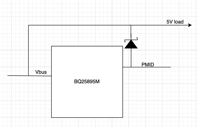
PMID output

Has to be supplied at

SYS output  (Buck converter) via

Input 5V supply or via

Backup battery in the absence of

Input supply Voltage.

required to power SYS and PMID 

in the absence of 5V Input supply.

For this purpose I have chosen 3 IC and I had a few questions regarding their functionality.

  1. BQ25895M
  2. BQ25620/BQ25622
  3. BQ25611D

Requirements:

1) The SYS output voltage and PMID should be supplied by Input source in the presence of Input source and also charge the battery.

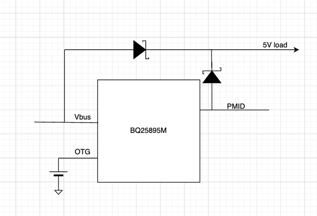
2) In the absence of Input source, the SYS as well as PMID should be provided by the backup battery.

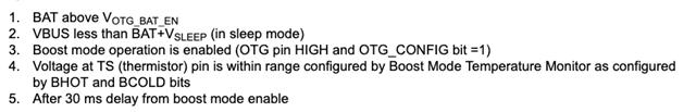
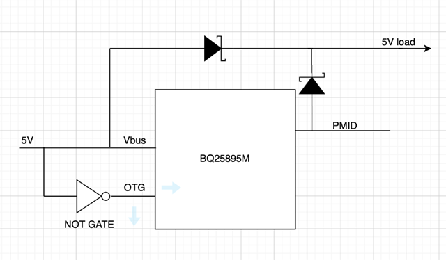
3) IC should be capable of detecting the presence and absence of Input source and automatically Boost the voltage at PMID in the absence of Input source and turn off boost when the Input source comes back.

The questions are as follows,

1) Are all of these IC's capable of Boosting the voltage (OTG functionality) in the absence of Input supply voltage while maintaining the SYS voltage (Buck Converter) at the same time? (The IC should be able to maintain SYS voltage and also Boost voltage with only backup battery as the source.)

2) Is there a automatic detection for the Input source so that the boost mode activation and deactivation is automatic? When the Input source (5V) gets turned off, the IC should automatically detect it and turn on boost mode and when the Input source comes back again, the IC should automatically turn off boost mode and simply connect Vbus to PMID via Power management. Can all the above mentioned IC's do this?

3) Which of the above mentioned IC's would be most suitable for the above mentioned use case with the mentioned requirements?

Thanks and Regards,

Srishtik.

  • Hi Srishtik,

    Device Specs to meet requirement:

    • For the BQ25895M
      • Can handle 5V input and has a max input current limit of 3.25A
      • Supports up to 5.5V OTG voltage regulation on PMID
      • Supports a max OTG current of 3.1A. 
      • SYSMIN ranges from 3.0V to 3.7V
      • Supports up to 6A continuous and 9A peak current discharge from the battery
      • Battery charge voltage regulation range is 3.84V to 4.608V
      • Fast charge current can go up to 5A in steps of 64mA
    • For the BQ25611D
      • Can handle 5V input and has a max input current limit of 3.2A
      • Supports up to 5.15V OTG voltage regulation on VBUS
      • Supports max OTG current of 1.2A
      • SYSMIN ranges from 2.6V to 3.7V
      • Supports 6A RMS discharge current from the battery
      • Battery charge voltage regulation range is 3.494V to 4.51V
      • Fast charge current can go up to 3A in steps of 60mA

    The OTG current will depend on the SYS load conditions. Also note that the SYS load is limited by the max discharge of the battery. Both chargers support NVDC architecture which means that the SYS voltage is held to SYSMIN when the battery is lower than SYSMIN in charge mode. When the input supply is disconnected, the SYS voltage will be slightly lower than the battery voltage due to the drop across the BATFET.

    1) For both chargers, the SYS output voltage will be supplied by the input source when the adapter is connected. In OTG mode, SYS can be supplied by the battery. We do not recommend loading the output PMID during forward mode. If you wish to do so, place the load before the reverse blocking FET so that the input current limit is not exceeded. 

    2) The BQ25895M does have automatic switching between OTG mode (boost mode) and charging mode (buck mode). When the adapter is disconnected, the device will operate in OTG mode and boost voltage from the battery to PMID. When the adapter is connected to VBUS, the device will switch to charging mode (buck mode). Removing the adapter again will cause the device to switch back to OTG mode.

    The BQ25611D does not have the automatic OTG detection since OTG mode output is at VBUS for this device. OTG current regulation is clamped by the RBFET so it is recommended to use VBUS as the OTG output. Connecting the adapter to VBUS during OTG operation will not switch the device to charging mode.

    3) My colleague will get back to you with more information on the BQ25620 / BQ25622.

    Regards,

    James

  • Thanks James for such quick reply.

    I had few more things to clarify.

    1) When Vbus is turned off:

        1. How is the detection being done?

        2. What are the steps to be taken to turn on boost converter? Is there any software dependency?

    2) As you mentioned it is not recommended to load the PMID during forward mode, I have come up with a circuit to avoid it.


         Using this we can supply 5V load via Vbus without loading the PMID FET. In the absence of Vbus, the PMID output is connected to 5V load

        via schottky diode (very low fwd voltage drop).

        1. Will this approach work?

        2. How will the detection of Vbus work? since now the PMID output is also available at Vbus via schottky diode.

        3. Or whether connecting 5V load directly at PMID without schottky diode  is the way to go?

            The maximum current drawn by 5V load is 100mA. Would the IC not be able to handle 100mA as you mentioned loading is not recommended?

    3)  When Vbus is back

        1. How does the IC detect that Vbus is available again?

        2. Are there any steps followed to turn off the boost converter? Is there any software dependency?

    4) As per my understanding, in the absence of Vbus,  Vsys = Vbat ( considering the voltage drop accoss BATFET), The battery is directly connected to SYS via BATFET and not buck converter.

    Thanks,

    Srishtik.

  • Hello Srishtik,

    Please see my comments below. I assume we are talking about the BQ25895M as it will switch automatically. I did notice you can switch from charging to OTG on VBUS on BQ25611D, but not back to charging when attaching the adapter. Here you are shorting two power supplies (the output of the convert and the input supply).

    1) As long as OTG and Charge bits are both enabled, the device will start OTG when removing input and start charging when plugging in the adapter. However, when plugging in the adapter the device runs through input detection as shown in 8.2.3.3 Input Source Type Detection. Please note to not load PMID while in charging mode.

    2) This setup should work. Please test according to your application. There will be no connection from VBUS to PMID only PMID to VBUS. When in forward charging mode PMID will be less than VBUS and the diode will not conduct. When PMID is greater than VBUS (OTG) the diode will conduct to the 5V load. When VBUS is powered again Input Source Detection will be run. Again, we do not recommend loading PMID in forward charging mode.

    3) Please see 8.2.3 Device Power Up from Input Source. The device detects when VBUS is plugged in. To turn of the boost converter you need to disabled OTG.

    4) The path with battery only goes from VBAT to VSYS to the converter to PMID (if using OTG). With no OTG the path is VBAT to VSYS.

    Regards,

    Mike Emanuel 

  • Thanks Mike for such a fast reply.

    I have come up with a circuit and I want to clarify a few things.

                                            FIG 1

    1) I have added a second schottky diode so that Whenever boost mode is enabled, the PMID voltage is not availbale at Vbus so that we know for sure that Vbus is detected only when there is Vbus is present and not due to the Boost converter output being present at Vbus. Is this fine?

    I have connected the OTG pin to battery directly so that OTG is always enabled and also in software we set the OTG bit to 1.

    As you mentioned OTG turn on is automatic in BQ25895 pertaining to a few conditions as mentioned below,

    2) What I want to know is whether the Boost mode will turn Off when any one of the condition fails? What I want to achieve is, when the Vbus is detected or comes back again, the second condition Vbus < BAT + Vsleep fails (As Vbus = 5V and BAT max voltage is 4.1 V) and the Boost converter is disabled failing to maintain the required conditions for OTG?

    OR ELSE:

                                             FIG 2

    This is the another circuit which employs a NOT gate.

    When Vbus is present, The output of NOT gate is logic LOW and OTG is diabled.

    When Vbus is absent, the output of NOT gate is HIGH and OTG is enabled. (OTG bit being set to 1 always and NOT gate  being powered with battery).

    3) Would this circuit be able to achieve automatic Boost converter enable and disable?

    4) Which circuit would be able to achieve automatic enable and disable of Boost converter without software dependency? FIG 1 or FIG 2?

    Thanks,

    Srishtik

  • Hi Srishtik,

    I will answer your comments in order:

    As a side comment please keep in mind the approximate 40 ms delay for turning on OTG.

    1) Please note if you only plan to load 50 to 100 mA of current from PMID in forward mode this may work without the Schottky diodes. However, you just need to make sure you provide enough input current limit so that this load does not put the part into IINLIM prematurely. However as we have not tested this please test according to your application.

    2) For i) If the battery is not above the VOTG_BAT_EN the OTG will turn off.

              ii) If an appropriate adapter is plugged in charging will start and OTG will stop.

             iii) If either the bit or the pin voltage are changed  OTG will stop.

             iv) If the TS voltage is out of range OTG will stop.

    3) This will allow switching between the modes, albeit there will be the delay as mentioned in the top of the post.

    4) The OTG bit is enabled by default. Removing the input will cause the device to go into OTG. Reapplying the input will cause device to exit OTG. Please abide by the checklist from the datasheet for boost operation enable.

    Please note we have not tested the operation of drawing a PMID load with charging enabled. We will not be able to provide support for such operation.

    Regards,

    Mike Emanuel

  • Thanks Mike for the above answer. It solved all my doubts regarding BQ25895.

    Thanks for such quick response. We can close the thread now.

    Regards,

    Srishtik.