This thread has been locked.

If you have a related question, please click the "Ask a related question" button in the top right corner. The newly created question will be automatically linked to this question.

LM5013-Q1: Output Voltage Going Over Voltage Set By Feedback Circuit

Part Number: LM5013-Q1
Other Parts Discussed in Thread: LM5013

I'm having issues with a 12V power supply I designed. 

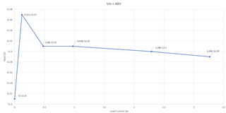
For testing I've got Vin set to 49V and with no load; I'm getting ~12.3V out.  With a 1A load; I get 13V out.  Also, the output voltage under load seems to be tied to the input voltage, because if I change my input voltage from 49V to 57V, the output voltage goes up to 13.1V.

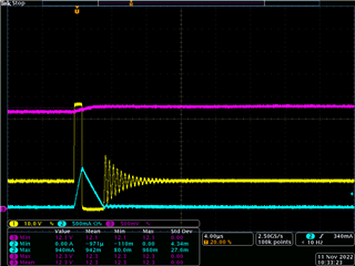
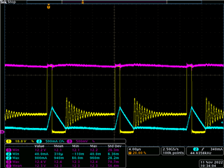
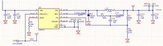
I have a feeling my issue is with the Type 3 ripple generation circuit, because when I remove this circuit, the output voltage stays constant at the 12.2V that it is supposed to be, but it is also pretty noisy (over 600mV of RMS ripple voltage at the output).

Here is the schematic for my circuit:
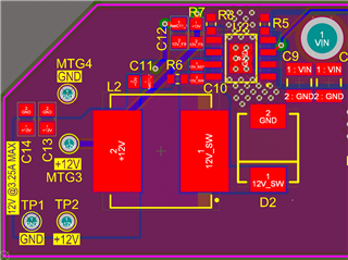
Here's the layout:

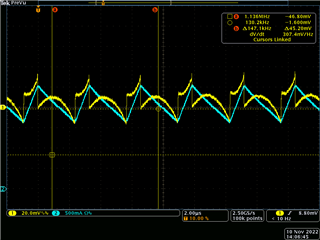
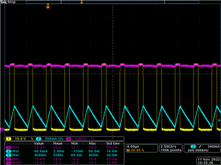
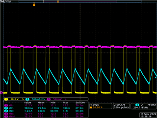
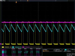
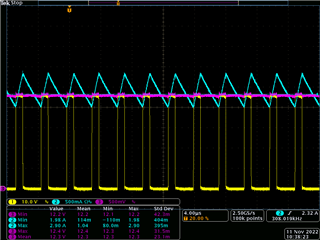
Here's the waveform of the inductor current (blue) and switch-node voltage (yellow):

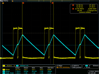
A few things I'm unsure about from the waveforms:

1. What could be causing the controller to turn off the in the middle there?

2. It looks like the frequency is actually 155kHz, even though the resistor setting should have it at 300kHz, am I looking at the waveform wrong?

   - to get 300kHz, I used the equation, fsw = (12(V)*2500)/(100(kΩ)) = 300(kHz)

Is there something obvious that I'm missing with my design? 

  • Hello,

    The waveform you show demonstrates insufficient ripple injection.

    The SW waveform shows irregular pulsing which is a characteristic of this behavior...the the comparator is false-tripping due to insufficient in-phase injection voltage ripple (w.r.t. inductor current ripple).

    My suggestion is you copy the ripple injection network: R6, C11, and C12 (on your board) with similar components contained on the LM5013-Q1EVM. The power condition of that EVM is a perfect match of yours. You can find the EVM userguide on the website or via google search.

    Yoou should see constant frequency operation at 1A load, with output ripple <<50mV. 

  • Thank you for the quick response!

    I took your suggestion and copied the values used on the demo board (including the feedback resistors) - but didn't see much of a difference.  I was still getting the glitch while the inductor was supposed to be charging.

    Reading through SNVA874 (Stability Analysis and Design of COT Type-3 Ripple Circuit), the exact scenario I was seeing with the double pulse was discussed and it suggested it had to do with an out-of-phase ripple which could be dealt with with larger output caps.  So I doubled my output cap to use 2x 47µF instead of the original 2x 22µF and that fixed the glitch, and the voltage is now stable, but my Vout is still higher than it should be - based on my feedback resistors. I'm measuring 12.2-12.3V whether there is a load or not, but with now using 453k & 49.9k feedback resistors - I am expecting the output to be closer to 12.1V.  Is this just 

    Could the slightly higher voltage be due to tolerance of the LM5013 or could still be caused by an issue with the ripple injection network being out of phase of the inductor?

    Here's a measurement I took of the FB pin (yellow) and the inductor current (blue).  Is this what I should be seeing on the feedback pin?

    Thanks!

  • Hello, you are welcome.

    I agree, I would expect closer to 12.1V as well.

    With injected voltage ripple much greater than the capacitive ripple to achieve stability (no false firing of on timer), you could potentially decrease your line reg figure, but you report that you do not see any variance over loading with keeping Vin fixed?

    With keeping Vin fixed, measure across the output cap if you can at min and max load.

    You should see something similiar to fig 6-2 in below datasheet.

    https://www.ti.com/lit/ds/symlink/lm5013-q1.pdf?ts=1668128645158&ref_url=https%253A%252F%252Fwww.google.com%252F

    If you are not, let us look at the corresponding SW and Vout waveform.

  • Thanks again for your quick response!

    I was definitely incorrect in saying that the output voltage doesn't change with respect to the load.  I took some measurements, and the output voltage does indeed change between min/max load.  Here is a graph of the data that I took at various loads:

    It's not exactly as flat as Figure 6-2, but it makes a similar jump between no load and a small load.  

    Does this look like what I should be expecting?

    Since you mentioned possibly looking at the SW and Vout waveforms, I went ahead and added those below in case there is something in them that stands out. (Yellow = SW-Node, Blue = Inductor Current, Purple = Vout with 10V offset)

    0A Load:

    0.123A Load:

    0.480A Load:

    0.978A Load:

    2.289A Load:

    3.265A Load:

    Thanks again for your help!

  • Hello Jacob,

    Your load regulation curve seems reasonable, as does the general control behavior.

    DC accuracy would be related to the average voltage on FB, as well, the gain of the feedback divider.

    My gut reaction is I believe something is being overlooked on the feedback divider.

    Email me at m-beck1@ti.com

    Ill see if I can get you an EVM for you to do A-B comparison if you like?