This thread has been locked.

If you have a related question, please click the "Ask a related question" button in the top right corner. The newly created question will be automatically linked to this question.

TPS65150: Noise on AVDD

Part Number: TPS65150

Hi,

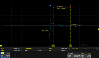
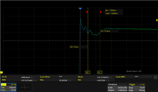
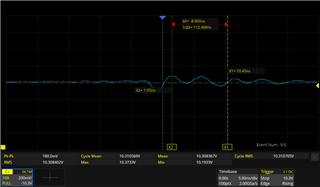
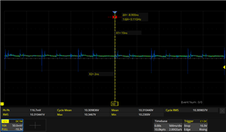
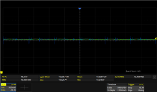
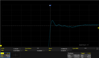
I have same problem as user6371168 (https://e2e.ti.com/support/power-management-group/power-management/f/power-management-forum/937718/tps65150-tps65150) with noise on AVDD. Noise is bigger with no load. It's better without load, but still significant. After reading support by Liaqat Khan in this thread, I redesigned my PCB, but problem is still here.

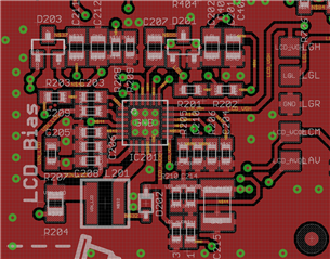
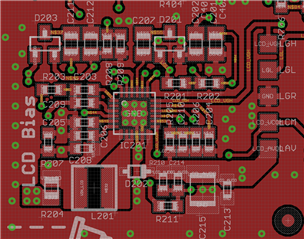
First PCB has only 2 layers of copper with one ground. 2nd redesign has 4 layer (1st signal + ground, 2nd ground, 3rd power, 4th signal + ground) and separated wiring of ground (power ground and analog ground) connected in one point with 0R resistor. Same issue on both board. So maybe is there problem with components...

Please see attachement for schematics and layouts.

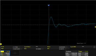
I've tried two types of diodes (D202) on AVDD. 1st cheaper TS4148 RYG and 2nd more expensive, faster PMEG3010CEJ on both design of PCB, but with no effect.

Don't know where the problem is... Thanks for support.

TPS65150.zip

  • Correction: It's better with load, but still significant.

  • Hi Marvin,

    Could you please share your waveforms plot?

    BR

    Patrick

  • Hi Patrick,

    please see attachement with all files. I add to ZIP archive the screenshots with waveforms. All screenshots are the same, but with variant timebase settings. Peaks correspond to the switching frequency (check timebase).

    Measured with SDS2204x oscilloscope and 200 MHz calibrated probe on testpoints LAV and LGD (you can see it on screenshots) with "paperclip method" (spring on probe - for small ground loop).

    Thanks

    2555.TPS65150.zip

  • Correction again... not LGD, but LGR testpoint.

    LAV testpoint = AVDD voltage (set to 10,38 V by calculations + tolerances)

    LGR testpoint = GND (ground potential).

    By the way, it is a pity that this circuit does not have any Enable or Shotdown input to deactivate the whole circuit.

    I attach the datasheet for the display used.

    APEX___TWVK700RETR40N_RevB.pdf

  • Hi Marvin,

    Are these waveforms captured with 2 layers PCB or 4 layers PCB?

    BR

    Patrick

  • Hi,

    these waveforms are captured with 4 layer PCB, but it looks same as in 2 layer PCB.

  • Hi Marvin,

    Is there any difference between 2 layers PCB schematic and 4 layers PCB schematic? I only find the difference of CTRL pin connection.

    BR

    Patrick

  • Hi Patrick,

    yes... the CTRL input and ground connection wired by R207 resistor with 0R value. Components are same. I've tried cheaper TS4148 RYG and faster PMEG3010CEJ on both design (2 and 4 layers), but with no diference.

    I think there is either a problem with the components or a bug in the schematic that I can't see.

    One thing is different from the schema... I forgot to mention that. FDLY is not connected by capacitor, but by resistor 0R to Vin to disable Fault Delay. It is a component C209 - there is no capacitor, but physically there is zero resistance. This is done in both design (2 and 4 layer).

  • Hi Marvin,

    What's the output capacitance of AVDD? it's not clear to see on your schematic.

    And have you tried to disconnect VCOM input with AVDD? I noticed the VCOM is supplied with AVDD.

    BR

    Patrick

  • Hi Patrick,

    I accidentally marked the answer as the solution... can it be reverted?

    Sorry for bad resolution in schematic... Please see PDF in attachement. Output capacitors are 22uF + 1uF (same as evaluation board).

    VCOM output is not connected to AVDD but signal is generated by AVDD and resistor divider (R205 + R206) connected to IN pin. There is only op. amp. between IN and VCOM. I could try to unmount R205 resistor to disconnect it from AVDD on Monday. It's same connection as in eval board, but with diferent values of components.

    Thanks

    TPS65150 PDF schema.zip

  • Hi Marvin,

    That's fine, I'll continue supporting you.

    BR

    Patrick

  • Hi Marvin,

    I noticed that the ripple appeared every 800ns, means the frequency=1.25MHz. This is very close to the SW frequency.

    In your PCB layout, I also noticed that the SW trace is not so wide. This may cause voltage spike during switching. And you can measure the waveform of SW, I think you can find similar ripple in every period.

    My suggestions are:

    • Adding a snubber circuit
    • Optimizing the SW trace. Place inductor near the SW pin and place a wider SW trace.

    BR

    Patrick

  • Hi,

    I wrote about frequency of peaks 8 days ago: "Peaks correspond to the switching frequency (check timebase)." - so it's generated by coil. It corespond to duty cycle too.

    The note about weak links seemed good. So I strengthened the connections by external wire and tin (see picture with marked connections and photo) and measured AVDD again and unfortunately no change. I tried the behavior without R205 resistor. Again no change. Please see waveforms and images.

    In the next design I will strengthen the connections on the PCB, but whether this will have any effect, I don't know.

    Do you have any more ideas for modifications before I release the next draft to production?

    Thank you

    Modifications.zip

  • Hi Marvin,

    I still suspect this issue was caused by switching. I think you could try adding a snubber circuit based on ripple oscillating frequency before next PCB production. 

    BR

    Patrick

  • Oh, I forgot to test the snubber... I'll post waveforms tomorrow.

    I think we've completely misunderstood each other... It's clear that the source of the interference is the coil switching. That's what I was trying to imply in the introduction.

    Tomorrow we'll be wiser. I will follow this application report:

    e2e.ti.com/.../Minimizing-Ringing-at-the-Switch-Node-of-a-Boost-converter.pdf

  • Hi Marvin,

    That's fine, I'll wait for your waveforms. Hope the snubber can make improvement.

    BR

    Patrick

  • Hi Patrick,

    please see waveforms in text and in attachement. The files are in alphabetical order as I measured and edited them.

    There is some ringing on SW-GND, but problem seems with output tracing... The noise is much more pronounced on the testpoints than on the output capacitor. (SW does mean Switching signal from TPS65150, but measured on L201 right pad, GND measured on C215 down pad.)

    Description of the waveforms (as it is ordered):

    1) Measured SW-GND and added 100 pF to reduce ringing (~227 MHz) by half (to ~112 MHz):

    2) and 3) Measured SW-GND. Computed resistor (22R) was added and ringing was reduced (100 pF + 22 R). I tried to replace 22R with 16R, but it's exactly same. Left (2) and right (3) waveforms are same, but with diferrent X-Y config.

    4) and 5) Measured AVDD on testpoints (LAV and LGD). Left (4) and right (5) waveforms are same, but with diferrent X-Y config. It's looks exactly same with no PCB mofification).

    6) Measured AVDD but not on testpoints, but on output capacitor C215 - much better.

    I realized that the position of C213 was not correct and I simplified the layout of input-output supply and strengthened the joints.

    Original layout:

    Modified PCB layout without snubber for now. I will add it close to L201:

    If you have any other ideas to modification, let me know.

    Thanks for support.

    TPS65150 snubber test.zip

  • Hi Marvin,

    I noticed you re-placed C213 and wider the AVDD trace, the modified layout looks better from my side. 

    And have you sent me the waveforms of SW without snubber before? I didn't find it.

    BR

    Patrick

  • Hi Patrick,

    I forgot to make screenshot with no modification... here is waveforms without snubber and with snubber (100 pF + 22 R):

    Both waveforms was measured today. The result is slightly better, but there is still a margin for tuning.

    But I will do the final tuning on the next version of the board, because there are differently placed connections and there parasitic inductance and capacitance will be different. In a month or so I might have a product and will upload the final progress here.

  • Hi Marvin,

    SW waveform is better with snubber, but AVDD has no obvious improvement, so I think this issue might be related more about your layout of AVDD part.

    As you have modified the layout, let us see if there will be any improvement with new board.

    I'll continue supporting you, please upload test results here once you get them.

    BR

    Patrick