This thread has been locked.

If you have a related question, please click the "Ask a related question" button in the top right corner. The newly created question will be automatically linked to this question.

TPS2492: Unintended Overvoltage Lockout

Part Number: TPS2492

Good evening Rakesh, Good evening fellow forum users,

During testing with the TPS2492 I have come across an issue with the Overvoltage Protection of the chip and would like to ask you for advice, Rakesh.
For reference please find the schematic of the respective circuit below, which includes the design setpoints of the OV Protection.
8741.Schematic.pdf


When triggering the Overvoltage protection of the channel, the channel occasionally latches-off and will not turn on again when going below the limit (OV,falling), considering the hysteresis.
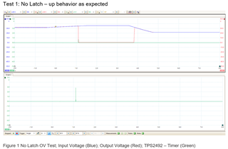
When trying to debug the issue I applied the following test sequence from a controllable voltage source

1) Start at Vin = 32V
2) Ramp Voltage to 36 V within 2s (trigger OV Protection)
3) Hold Voltage at 36 V for 2 s
4) Ramp Voltage down to 22V within 2s (go below OV,falling)
5) Keep voltage at 22V

In figure 1 you can see the regular expected behavior of the circuit. The Gate driver shuts down the channel when surpassing 35.4 V and turns it back on when falling below 33.1 V


In some cases for the same sequence the following (figure 2) happens: The Gate driver shuts down the channel, but does not restart when falling below OV,falling.

I measured the voltage on Ct for the latching case and surprisingly it hits 4V while going below OV,falling. As a consequence the channel latches off.


When zooming in on V(Ct) it is recognizable that Ct is getting charged with roughly the 27 uA you would expect during power limit/current limit event according to datasheet:
Datasheet P.8: The timer charges at 27 µA whenever the TPS2492/3 is in power limit or current limit and discharges at 2.7 µA otherwise


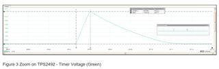
To exlude that the gate driver is actually switching at this point of time, I scoped the gate-source voltage of the Mosfet, but no turn on event of the Gate driver can be observed:


Now out of curiosity I tested the same sequence on an already latched-off channel and the following was the result:
Even for a latched-off channel there is some significant rise in V(Ct) when the OV surpasses OV,rising and falls below OV,falling.


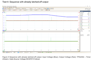
What causes this rise on V(Ct) and the consequential latch-off and how can we fix this problem?
In our application the latch-off is definitly not intended.

I appreciate your help. Please do let me know, if I can provide any additional info or do additional tests on the way to a solution.

Cheers

Konstantin E.

  • Hi Konstantin,

    Thanks for reaching out 

    The load at the output during recovery from OVP might be higher than the power limit setting 

    Can you test at no load or increase either power limit value or timer capacitance value  and check

    Best regards 

    Rakesh 

  • Dear Rakesh,

    Thank you for the quick answer. The above tests were all carried out with no load connected to the channel.
    In Figure 4 you can also see that the gate-source voltage is not increasing to the threshhold voltage of the MOSFET when reaching UVLO,falling .Therefore we know the gate driver is not trying to restart.

    Best
    Konstantin

  • Hi Konstantin,

    Thanks for the confirmation.

    There is no excessive output capacitance as well - right ?

    Can you test by increasing either power limit value or timer capacitance value

    Are you observing similar behavior on all the boards and units ?

    Best regards 

    Rakesh

  • Hi Rakesh,

    Sure thing. Is your assumption that we're in power limit while turning on?

    There is only the 1 uF ceramic capacitor at the output shown in the schematic, which with the dV/dt control of the gate is more than a factor 1000 below the capacity, for which inrush current could trigger the power limit during turn on.

    Also as mentioned in the post before, the gate driver is not increasing the gate-source voltage to the threshhold of the MOSFET - therefore we're not getting to the point where any mosfet drain current would flow. The channel is fully kept off.

    So far I have only tested with one board. I can confirm until next Tuesday if the issue shows on multiple boards.
    Do you have any other ideas at this point what could be the cause?

    Appreciate your help!

    Konstantin

  • Little update to the initial post:

    I by accident posted in figure 2 an image where the driver does indeed not latch off (-> see output voltage in red). Sorry about that.
    Below is the picture that actually corresponds to figure 2 where you can see the latch-off via the output voltage in red:


    The rest of the images posted were correct ones.

  • Hi Konstantin,

    Yes, I am expecting the device is entering into power limit mode during OVP recovery. Other than that, I don't see any reason for it not to recover.

    Please continue testing and confirm.

    If we are seeing similar behavior on other boards, we may need to get your units for debug.

    Best regards.

    Rakesh

  • Hi Rakesh,

    Bad news. The issue shows on 3 different boards and also in the PCB of a colleague of mine who has a slighty different peripheral circuit and completely different layout & board stack-up.
    I also tested on my board if the Circuit is able to turn on (by cycling the UVEN pin) at 33.1 V and that works successfully.


    This all points in the direction of an IC internal cause. Due to IP (& frankly speaking also component availability issues) we can't provide you with our own hardware. Are you able to recreate our schematic on a test board of yours and see if you can reproduce the error?

    Let us know if we can support the analysis in any other way. If you want to discuss outside of the forum feel free to write to my company mail provided in my account.

    Looking forward to your reply.

    Konstantin

  • Hi Konstantin,

    sorry to hear that.

    Let me cross-verify at our end as per your schematics. I have ordered EVM which I will get by mid next week. So I will be able to perform test by end of next week.

    If there is any mismatch then we can submit your units for failure analysis.

    Best Regards,

    Rakesh

  • Hi Konstantin,

    Just checking.. the application is aerospace. Have they exposed the part to any radiation before doing these tests. I want to double check the misbehavior as the result of that or not.

    Best Regards,

    Rakesh

  • Hi Rakesh,

    No worries - happy to answer all questions you might have.
    No the boards are fresh out from assembly, no exposure to radiation or similar.

    Best,
    Konstantin

  • Ok Konstantin. Uunderstood

  • Hi Konstantin,

    The device recovers as expected on EVM at my end. Please see below results

    Best regards.

    Rakesh

  • Hi Rakesh!

    Thanks for coming back to me with the results.

    In the plots the OV,rising value seems to be 48 V, the OV,falling 46 V therefore quite different to the values I tested with.
    Was the rest of the EVM adjusted to the values I used in my schematic?

    Also how many times did you repeat the test? Sometimes it took up to 15 tries to reproduce the error. I can't really tell what exactly affects the probability of it happening or not at this point.

    Best regards,

    Konstantin

  • Hi Konstantin,

    I have tested as per the EVM schematic. The recovery behavior is independent of OVP threshold.

    Since, it is not repeatable every time on your board.. it is challenges. Can you share the layout file for review. Is it possible to ship your board for debug.?

    Best Regards,

    Rakesh

  • Hi Rakesh,

    Which EVM are you using? The TPS2492EVM-003?

    Which V_prog value and Timer capacitor are implemented there? Could you adjust the corresponding components in the Eval board for V_prog and timer to match my schematic and retry to reproduce the issue with that? Otherwhise it won't be representative.
    Scoping the voltage on the timing capacitor would help aswell, to understand the behavior on the eval board.

    If you still can't reproduce it at this point I can try to reproduce it on the eval board we have at the company.
    I can send you my layout per e-mail if you could share me your address, but as mentioned we have two different boards (with different layouts & stack-ups - both designed by experienced layout designers) where the issue occurs.

    Sending our boards is not our preferred option due to component availability and also IP considerations. 

    Thank you for the help.

    Konstantin

  • Hi Konstantin,

    Yes, I used TPS2492EVM-003

    At no-load, OVLO recovery is independent of Vrog and timer setting. Since it is not recovered at no-load on your board, I suspect it as system/setup issue and not the device issue.

    Please evaluate on the EVM you have and confirm. 

    Best Regards,

    Rakesh

  • Hi Rakesh,

    Following up on your response I tested with your Evaluation Board TPS2492EVM-003 and could reproduce the issue there with essentially only one component changed.

    I tested with the following sequence:
    1) Start at 50 V
    2) Increase Voltage to 55 V within 2s
    3) Hold Voltage at 55 V for 2s
    4) Reduce Voltage to 50 V within 2s


    First to validate the sequence it was checked with the EVM in original state with C9 removed to excude the effect of inrush current:


    No latch as expected. Once C5 was changed to 780 pF the latch appeared. Note also how the timer voltage reaches 4V, which cannot be explained by actual power dissipation over the Mosfet.


    Once again to exclude the effect of any turn-off behavior, I tested in already latched-off state and even here the timer voltage unintentionally rises to 4 V.


    Consequently the behavior can neither be explained by the specific circuit design of us, nor the layout. This heavily points in the direction of a malfunction of the chip to me. You should be able to reproduce this behavior on your own EVM by applying the same changes as I did to further investigate.
    We have spent significant time on our side to exclude this is a specific issue with our design, therefore I would appreciate if Texas Instruments would match that effort and find a fast solution for the problem.

    Thank you in advance and looking forward to hearing back from you,

    Konstantin Edl

  • Hi Konstantin,

    Thanks for the update but that is strange.. Let me check the dependency of timer capacitor C5 on the recovery behavior.

    can you confirm that output capacitance C9 47uF is removed for all the test cases.

    Also, may i know the reason for using such low timer capacitor in your system.

    Best Regards,

    Rakesh

  • Hi Rakesh,

    Thank you for your comment.
    Yes I can confirm that C9 is removed for all the test cases. Find below an image of the setup as used:


    I agree with you, it should indeed not have any influence on the recovery behavior, this is why I see necessity for an investigation on TI side.

    As you see in figure 8 of my last post, there is even an increase in Timer voltage in the latched-off state of the chip, while crossing the OVLO,rising and OVLO, falling threshold (where the chip is neither trying to switch on or off). 

    The reason for the small capacitor is to stay within the Safe Operating Area (SOA) of the Mosfet during short-circuit turn-off. With V_prog at ~ 0.4 V (specified as the minimum by TI) and the current requirements of the channel by our side, this is the maximum capacitor value we can use.

  • Hi Konstantin,

    Thanks for the confirmation.

    Please allow sometime to work at our end as most of the team are on holidays. I could be able to get update by 6th Jan.

    Please continue evaluation on the other functions/ system testing.

    Best Regards

    Rakesh

  • Hi Rakesh,

    Hope you had a great start into 2023.
    Are there any any news about the topic? Did you manage to get an update here?

    Best regards,

    Konstantin Edl

  • Hi Konstantin,

    I am waiting for the update from my design team. I will check and reply you on Monday 

    Best regards 

    Rakesh 

  • Good morning Rakesh,

    Is there any news on the matter? When can I expect an answer here?

    Best regards,

    Konstantin Edl

  • Hi Konstantin,

    Apologies for the delay. Our design team was able to import all the related project files and analyzed the circuit to root-cause the issue. We are able to see the similar behavior in simulation as well and by design it is expected to happen with lower timer capacitors.

    During OVP event, the device runs an internal deglitch clock and starts charging external timer capacitor for one clock period. The internal clock period is 120us width (typ) and 160us (max). so, we need to select timer period > 160us i.e., Timer cap should be > 1.5nF.

    In general, customers set higher timer period >500us with large timer capacitor so we haven't seen it as concern.

    Please let me know if you have follow-up questions.

    Best regards 

    Rakesh 

  • Hi Rakesh,

    Thank you for your response and explanation. Appreciate it.
    I suppose a minimal capacitance will be added to the datasheet soon in that case ?

    Two follow up questions.

    Is that deglitch clock cycle run independent on how long the OV persists or will it be cancelled if the OV condition is removed within these 120us - 160 us? Our overvoltage events actually take significantly less time than the 120 us.

    Do you know the dependency of temperature on this clock cycle length ?
    A graph like this would be very helpful:


    Best Regards,

    Konstantin Edl

  • Hi Konstantin,

    Yes. we will take action to update on the minimum capacitance value in the data sheet

    The deglitch clock is of fixed pulse period which starts when OV triggers and runs independent of how long the OV persists. From design simulation and analysis, the team gave 160us as max value considering temperature and process variation.

    We won't be able to provide the graph you are referring for the clock cycle length.

    Best regards 

    Rakesh 

  • Hi Konstantin,

    I am closing this thread. Please feel free to post if there are any follow-up questions.

    Best regards 

    Rakesh