This thread has been locked.

If you have a related question, please click the "Ask a related question" button in the top right corner. The newly created question will be automatically linked to this question.

LP38512-ADJ: LDO failure mode: Vout = Vin. Vadj no longer constant at 0.5V but depends on feedback resistor value

Part Number: LP38512-ADJ
Other Parts Discussed in Thread: TPS7A7001, TPS7A57

Hi,

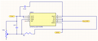
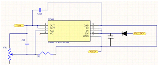
We configured this LDO as shown in the Typical Application circuit diagram.  

Vin = 5V

Vout = 3.3V typical

Maximum load current 500mA

R1 (feedback) = Trimmer Resistor (3296W-1-103LF)

R2 = 1kohm thick film resistor (RS73F1JTTD1001B)

Cin = Cout = 10uF ceramic capacitor (TMF325B7106KMHP)

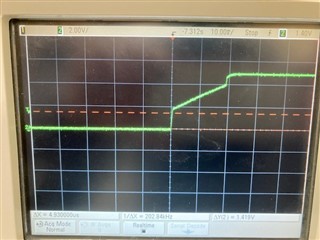
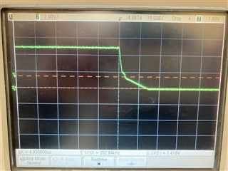
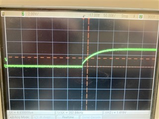
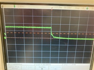
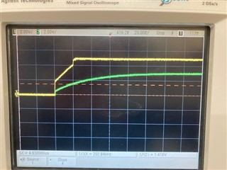
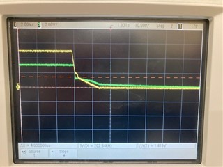
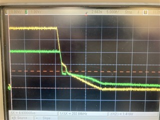
3 out of 5 boards tested at room temperature have the following behavior after a few days of usage.  Vout = Vin = 5V.  When we probed Vadj its value now changes with trimmer resistor, e.g. Vadj = 0.6V if R1 is set to 2.315kohm.  Vadj should be fixed at 0.5V.
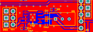
2-layer PCB

schematic

layout

  • Hi Frank,

    What was the operating condition during this period of time? Is the device operating at steady state? If so, what is the load current? Alternatively, is the device pulsed with load transients? If so, what are the specifications of the load transients? 

    It sounds like the pass FET was damaged somehow. Was the device regulating properly before leaving it for a few days? Was the device power cycled during this time?

    Regards,

    Nick

  • Hi Nick,

    This main LDO (same LDO broken on all 3 boards) provides ~3V to 8 other LDOs (same part number) and in turn those LDOs provide various DC bias voltages ranging from 0.8V to 1.2V.  The 3V output from the main LDO also drives 4 resistive dividers each followed by an op-amp follower for bias voltages below 0.5V.  

    The total current drawn from the 5V input to the main LDO is ~500mA (the power supply unit that provides this 5V is current-limited at 800mA).  The device is operating at steady state. None of the DC biases drive clocks.

    Yes, the device was regulating properly, and yes, we power cycle this board.  We typically turn off the PSU that powers this board at night, turn it back on in the morning.  One day the biases voltage from the resistive dividers were all wrong, then we noticed that the main LDO output is 5V.

    Some additional information: this particular power board design used to have TI TPSA7001s and I believe we never had this problem.  We switched to LP38512-ADJ due to shortage.  Not sure if there is any difference in terms of current protection on these two parts.

    The resistance looking into Vin of the bad part is 460kohms.  The resistance looking into the Vin of the good part is 880kohms.

    Thanks for your help,

    frank

  • Hi Frank,

    500mA is well within the specified range, and I don't think the power dissipation is excessive given that you have used an appropriate layout for the device with thermal vias. So for the steady-state operation this looks normal.

    Have you taken any waveforms of the power-up and -down? My next question would be whether the voltage waveforms are as well-behaved as you expect since the operating input voltage is relatively close to the upper limit of the specified input voltage range, and if there is some overshoot maybe it is getting damaged that way. TPS7A7001 has a slightly higher voltage rating (7V vs. 6V abs max for LP38512-ADJ), so that would support the idea that an overshoot is damaging the device.

    Regards,

    Nick

  • Hi Nick,

    The ENable of the LDO is hardwired to VDD on the PCB board, this input is connected to E3631A's +6V port (set to 5V) with current limit set to 500mA through header pins (where oscilloscope probe is connected to below).  The only capacitor at that node is the 10uF 0603 ceramic cap.  Power-up/dn is through turning ON/OFF the E3631A's Output On/OFF button.

    Input of the LDO (Power-up):

    Input of the LDO (Power-dn):

    Output of the LDO (Power-up):

    Output of the LDO (Power-dn):

    Thanks,

    frank

  • Hi Frank,

    These look pretty well-behaved. Can you capture one more scope shot of both the input and output of the LDO on the same waveform? I want to be sure that there's not a reverse voltage condition if the input falls much faster than the output. As far as I can tell from the scope shots you've provided this seems unlikely but it would be good to rule it out. 

    Have you done any further testing to try reproducing this failure? In my eyes the part is being damaged somehow, so it would be good to have some evidence to support this, or evidence that shows non-reproducibility; either would be useful. Maybe a good couple tests to start would be repeated power cycling and leaving the board powered without powering it down. Then if one fails and the other doesn't that could help suggest a problem. 

    Regards,

    Nick

  • Hi Nick,

    Channel 1 (Yellow) is LDO input, Channel 2 (Green) is LDO output.  Normal behavior on Power Up.

    During Power Down, it appears that the input voltage drops faster than output voltage, so there is some period where the output node is still discharging and the input voltage falls below output.  However, the maximum Vds is still less than 0.5V in reverse.

    Here is a "zoomed-in" picture, Y-scale at 1 V/div, 2V offset.

    Nick, I would like to get your suggestion on how to make this design more robust at the board-level, e.g. adding Schottky diode (for reverse current), adding more capacitor at the input (so it discharges slower on power down?), adding diode at the input (could this be ESD-related)?  

    Thanks,

    frank

  • Hi Frank,

    Adding more input cap could help, but if there is a large discharge path for the input caps to discharge upstream then it won't help as much. However, adding a diode in front of the input caps would prevent this upstream discharge so that when the main supply falls, the input to the LDO doesn't fall with it immediately. You can also add an extra load resistor to the output of the device to help the output discharge faster. This load resistor doesn't have to be much; it could be ~1kΩ and that would help the output continue to discharge once the load devices stop pulling current. 

    Alternatively, you could use a newer device that has more protection features. If you would be interested in exploring this option I can help find a suitable device. 

    Regards,

    Nick

  • Hi Nick,

    I am interested in newer devices with more protection features . May I ask what "LP" model number stands for (looking at Iq, it does not appear to be lower power than TPS series, e.g. comparing TPS7A7001 vs. LP38512-ADJ).  It does not appear to be lower cost.  Is it a National Semiconductor part, but with LP instead of LM? 

    I am interested in LDOs with Vin_max of 6V (nominal 5V), Vout programable down to at least 0.5V.  

    Thanks,

    frank

  • Hi Frank,

    I don't know if "LP" stands for something specific, but yes this is a National Semiconductor device. 

    I see. The 0.5V output voltage is definitely a limiting factor for this; we only have a handful devices that meet this requirement. TPS7A57 is the best device, but also by far the most expensive. Next is TPS7A8401A. The other options are TPS7A7001/2 but it sounds like you have already looked at these devices. 

    Regards,

    Nick