This thread has been locked.
If you have a related question, please click the "Ask a related question" button in the top right corner. The newly created question will be automatically linked to this question.
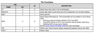
The data sheet of the TPS22810-Q1 contains a table with different values for the CT cap.
In the table there are also rise times for CT = 0 F
Also at different positions in the data sheet there is either the CT completely ommited (e.g. Fig 19 and 20) or specified as CT = 0 F (e.g. Fig. 28 and 31).
However, in section 8.3.4 Adjustable Rise Time (CT), the CT capacitor is not specified as optional part of the circuit (such as for the Cin and CL).
I have 3 TPS22810-Q1 in my design
#1: Vin 3 to 18 V, Cin= 22uF, CL= 0 F, CT= 0F
#2: Vin 5.3 V, Cin= 1 uF with uF, CL= 0 F, CT= 0F
#3: Vin 3.3 V, Cin= 1 uF with uF, CL= 0.1 uF, CT= 0F
So just to be sure,
Q1: I assume the TPS22810-Q1 can function properly with CT pin not connected and floating as implemented in my current design? Or is using a CT mandatory...?
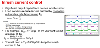
Q2: In Fig. 28 and 31 of the data sheet the inrush current is shown for CL = 22 uF and for 100 uF with CT = 0F. I am wondering what is limiting the inrush current in these cases to around 1.8 A and 7.5 A respectively?
Thank you,
Michael
Hello Michael,
The device controls the output slew rate to limit inrush current. The CT pin can adjust that slew rate to slow it down by adding capacitance from it to GND. As you can see in the pin functions table on page 3 the CT pin can be left floating, or you can place a capacitor to GND.
In the slide below you can see how you can calculate your inrush current using your rise time. You can also see in the scope shot the difference between an output with slew rate control and without (The large spike in current is when the inrush current isnt being controlled through the slew rate).
Regards,
Kalin Burnside
Dear Kalin,
tank you for your reply and explanation. I understand.
My problem is that I really have to struggle with real estate on my PCB and if possible would prefer to omit the CT caps.
Also for the devices on the TPS22810-Q1 output the lowest possible slew rate would be the best...
As said I have three TPS22810-Q1 in my design. the first one is connected directly to the main power supply for which a large inrush current should not be problematic.
The other two have another device in front:
TPS22810-Q1 #2: after XC8109AC10ER-G with current limit set to 400 mA and 11 uF capacitance at the output, i.e. 11 uF at the input of the TPS22810-Q1 #2
TPS22810-Q1 #3: NCP163ASN330T1G 3.3V high PSSR LDO with 250 mA nominal output and 1uF capacitance at its ouput, i.e. 1 uF at the input of the TPS22810-Q1 #2. Here I place a Cout with 0.1uF at the TPS22810-Q1 output to smooth the voltage somewhat. The NCP163ASN330T1G is short circuit protected with output short circuit duration being unlimited while the NCP163ASN330T1G itself limits Isc to 690 mA
So taking all this together I would hence think that in case of TPS22810-Q1 #3 operating without CT should be fine...
And as long as the load capacitance of the load on TPS22810-Q1 #2: after XC8109AC10ER-G with current limit set to 400 mAdoes not exceed the 11 uF of the capacitance placed between TPS22810-Q1 #2 and XC8109AC10ER-G, current through XC8109AC10ER-G should not exceed the set 400 mA limit and induce an overcurrent shut-down of the XC8109AC10ER-G right?
What are your thoughts here and would you recommend placing CTs in this context?
Thank you and best regards,
Michael
Hello Michael,
Since your load doesn't have any significant capacitance, and the current is limited upstream then I don't see any issues at all with leaving the CT pin floating for your use cases.
Regards,
Kalin Burnside