- Ask a related questionWhat is a related question?A related question is a question created from another question. When the related question is created, it will be automatically linked to the original question.
Hi.
Please, could this be revised by an engineer of Texas Instruments?
I'm open for tips and suggestions.
The initial schematic is attached.
DESIGN
Input voltage: 5.25V max, 4.75V min (5V +- 5%, input voltage is 5V typ)
Charge current (typ): 2.5A
Battery nominal voltage: 3.7V (Li-ion)
Battery floating voltage: 4.2V
Temperature protection: yes, using thermistor 103AT-2 from Semitec
SAFETY TIMER
Fast charge safety timer = 15h min, 20h typ, 24h max, shown at the end of page 10 of datasheet. 15h * 2.5A * 0.9 = 33.75. Ok, we will use a battery/polymer with a maximum of 20Ah capacity, in the worst case. If later we reduce the charge current to 2A, 15h * 2A * 0.9 = 27, it's also ok.
SETTING THE VOLTAGE OF THE BATTERY
According to the datasheet, "For a 1-cell 4.2-V battery, R1 = 562KR and R2 = 200KR are recommended".
VFB = 1.1V
1.1+1.1*(562/200) = 4.191V
562K 1% 0603 and 200K 0.1% 0603
CHARGE CURRENT
Charge current of 2.5A
I_chg (A) = K_ichg (Aohms) / R_ichg.
K_ichg is typically 40000 Aohms
R_ichg= K_ichg / I_chg
R_ichg= 40000 / 2.5 = 16K ohms
R_ichg commercial = 15.8K ohms
Ichg (typ) = 40000 / 15800 = 2.53A
INDUCTOR SELECTION
The Inductor chosen has 1uH, because VBUS (Vin) is < 6.2V) [page 22 of the datasheet]. It is considered a maximum input voltage of 5.5V.
The inductor ripple current IRIPPLE depends on the input voltage (VVBUS), the duty cycle (D = VBAT/VVBUS), the switching frequency (fS) and the inductance (L).
The maximum inductor ripple current occurs when the duty cycle (D) is 0.5 or approximately 0.5.
I_ripple = ( Vin * D * (1-D) ) / (fs * L)
Iripple = ( 5.5 * 0.5 * (1-0.5) ) / (1.2*10^6 * 1*10^-6) = 1.14A
I_sat = Ichg + 0.5*Iripple
I_sat = 2.53 + 1.14 = 3.67A
Inductor chosen: Inductor microHenry, SMD, 1uH, +-20%, 5.8A current rating, 8.5A saturation current, shielded, 26mOhm max, -40°C ~ 125°C, 4.2 x 4.2 x 2mm, PA4332.102NLT (Pulse Electronics)
BATTERY TEMPERATURE PROTECTION
Project requirement: 0°C to 45°C
The datasheet gives the values for this situation.
RT1 = 4.527K (commercial = 4.53K 1%)
RT2 = 23.26K (commercial = 23.2K 1%)
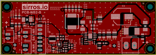
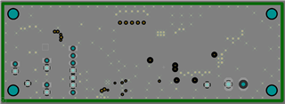
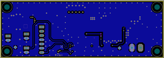
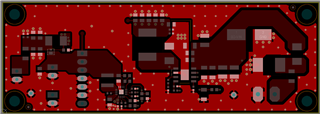
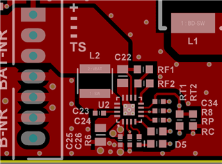
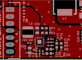
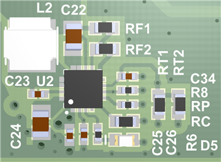
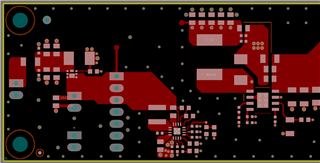
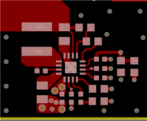
CURRENT LAYOUT
Do you think the layout is ok?
Regards,
Jeferson Pehls.