


Other Parts Discussed in Thread: CSD18514Q5A, CSD17573Q5B, CSD18540Q5B
Dear Colleauges,
We are between a rock and a hard place with this chip.
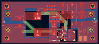
This is our second attempt after, in the first one we had problems with VCC regulation. We now redesigned the converter with the help of WEBENCH, manually verifying value selections. The board was also rerouted following the official layout guidelines of the datasheet.
Please look at the attached design, and WEBENCH document. Our schematic is a simultaneous design of a 19V and 28V optimized design which share a PCB.
Neither of them works.
On both designs bottom mosfets are driven to be an effective short (as observed in our input power measurement setup) after a short grace period, and they overload the input supply as burning to a total short. After the mosfet is removed, the chip boots up and provides the expected 5V clean VCC and 1V reference, and the feedback voltage on the TRK pin is totally right. If a new mosfet is placed, it burns out just like the previous.
Could anyone explain this behaviour?
3252.power-module-boost.pdf19v.pdf28v.pdf
All of our chips and parts came from Mouser.


