This thread has been locked.

If you have a related question, please click the "Ask a related question" button in the top right corner. The newly created question will be automatically linked to this question.

P Channel MOSFET

Other Parts Discussed in Thread: CSD25404Q3, TINA-TI, LM7480, CSD18536KCS, LM5060, CSD18536KTT, LM7480-Q1

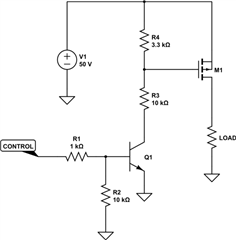
Need to Trigger PMOS at 48V for a Source switching circuit, can you help. I was looking iinto Voltage devider as a trigger 

  • Hello Suhas,

    Thanks for the inquiry. A P-channel MOSFET is turned on by pulling the gate negative with respect to the source making it simple to drive. Limiting VGS to less than its absolute maximum rating is required in an application where the source is connected to a voltage higher than this rating. A resistor divider or zener diode and resistor may be used to limit the voltage applied between gate and source when turning on the device. An example using an NPN transistor with a divider is shown below. A N-channel FET could be used instead of an NPN transistor.

    Best Regards,

    John Wallace

    TI FET Applications

  • Thank you John. I am using this circuit for now. My Intended current is 100A. I need to switch between two source based on availability. So using Two such circuits should be fine right?. Is that the conventional method?. 

  • Hello Suhas,

    Thanks again for the inquiry. Most OR'ing applications use N-channel MOSFETs with an OR'ing controller. P-channel FETs are typically larger and higher cost than an N-channel device with the same on resistance. The OR'ing controller includes the logic, timing and charge pump to drive N-channel FETs. I think you can use two of these circuits in your application. You would have to control the sequencing of the FETs and I would recommend adding a place holder for a capacitor from gate-to-source on each FET in case you want to slow down the switching. Let me know if I can be of further assistance.

    Thanks,

    John

  • I have looked into the oring controllers but most of them that work at 50V always take the higher voltage path to the load. I am looking for a solution where my primary supply is always connected to the load and In case of primary failure the auxiliary should kick in. So in a way controlled oring. Or Priority oring. 

  • Hi Suhas,

    I believe what you are describing is power muxing. TI has some devices for power muxing but nothing that can handle the high current. I believe you should be able to use the P-channel FETs and associated circuitry to accomplish this. Please let me know if I can be of any further assistance.

    Thanks,

    John

  • Okay Thanks John. So you are saying that the Voltage devider circuit will work fine for the pMOS switching for 2 Sources. Right?. I just need a validation that it will work .

  • Hello Suhas,

    I cannot guarantee that this circuit implementation is going to work in your application. I have some concerns including selection of a P-channel FET capable of blocking 50V and carrying 100A of current without incurring excessive conduction loss. You will probably need to use at least a 60V FET for margin and multiple devices in parallel to reduce the conduction loss and spread the heat over multiple packages. TI does not make any P-channel FETs for this application. Also, keep in mind that MOSFET on resistance has a positive temperature coefficient and will increase as the device heats up due to the conduction loss. Finally, be aware that you could get reverse current flowing thru the body diode of the FET that is OFF if the output is higher than input voltage source to the FET. To prevent this you may need to have two FETs back-to-back to block the reverse current. In turn, that means you will have double the conduction loss because there are two FETs in series. As I mentioned previously, for the same on resistance, a P-channel FET will have a larger die size and be more expensive than a comparable N-channel FET. I'd highly recommend simulating this circuit to better understand how it is going to work in your application. I have created a scaled down TINA-TI simulation using the CSD25404Q3, -20V PFET and it does show reverse current flow thru the FET that is off when the output voltage is greater than the input source voltage to that FET. I'd be happy to share with you if you are interested.

    Best Regards,

    John

  • Thank you John. I had already simulated this and have connected PMos back to Back and connected 3 sets in parallel for the resistance reduction. 

    From what I am incurring for the current global scenario are PMOS getting outdated for such applications. If So can I get a good circuit with NMOS. 

    The thing is we are updating an existing circuit which already had PMOS. Initially it was for 24V and we did not have a problem with off the shelf drivers. But when it came to 48 V it's hard to find drivers and also actual working circuits. 

  • Hi Suhas,

    You can probably use a hot swap controller such as the LM5060 or an ideal diode controller like the LM7480 in your application. Both include a charge pump to drive N-channel FETs. This would allow you to use a TI N-channel FET. If you can use a 60V device, our lowest on resistance device is the CSD18536KTT (D2PAK) or CSD18536KCS (TO220 which can be attached to a heatsink). TI also has 80V and 100V FETs in these packages as well. I am not responsible for the hot swap and ideal diode controllers. If you are interested, I can reassign this thread to the applications team responsible for those devices.

    Thanks,

    John

  • We are looking at 100A . Will those components suffice

  • Hi Suhas,

    A single FET will not handle 100A as the power loss would exceed 20W. You would need to parallel 2 or 3 devices in order to handle 100A. We have a load switch FET selection tool available at the link below. You can use this to estimate the conduction loss in the FET. It does not allow for paralleling but you can simply divide the current by the number of parallel FETs. With two FETs in parallel, the estimated conduction loss is ~5W per FET. With three in parallel it drops down to ~2.2W per FET. The tool uses the maximum on resistance specified in the MOSFET datasheet and also calculates the increase in on resistance based on the junction temperature. I assumed TJ = 75°C for these estimates.

    Can you share the part number of the P-channel FET you are using?

    https://www.ti.com/tool/LOAD-SWITCH-FET-LOSS-CALC

    Thanks,

    John

  • So there arent any pMOS drivers at 50V . Can i get any samples for the NMOS drivers. if possible\

  • Hi Suhas,

    I'm not aware of any PMOS drivers. Samples can be ordered from the TI store on TI.com.

    Best Regards,

    John

  • SUP90P06-09L-E3 is the MOSFET that we re currently using

  • Switching.pdf

    I am using this circuit for the switching 

  • Hi Suhas,

    Thanks for providing additional information. Your schematic looks OK but you may want to consider adding a place holder for a gate-to-source capacitor in case you want to slow down the switching. Also, I would recommend a small value gate resistor (5 - 10Ω) for each FET. This is best practice when paralleling FETs as explained in the application note at the link below. The conduction loss (I²R) with the P-channel FET you are using is going to be 50W (TJ = 125°C) to 63.3W (TJ = 175°C) per 3 parallel FETs and double that amount for back-to-back FETs. I do not know if 100A is continuous or if that is peak and the continuous current is lower but that is a lot of power to dissipate. By comparison, if you use the CSD18536KCS in TO220 with an ideal diode controller such as the LM7480, you can reduce the loss to around 10W - 12W per two parallel FETs. Double that amount for back-to-back devices. The LM7480 has an integrated charge pump and can drive back-to-back N-channel FETs. It includes some protection features and has an enable pin which allows you to select the preferred power path.

    https://www.ti.com/lit/an/slpa020/slpa020.pdf

    Best Regards,

    John

  • the current is 65A Total

  • can you share the schematic also ?

  • Can you send me the Simulation file for LM7480, with the circuit u mentioned. When i see the Datasheet its not mentioned that it can be used parallely.

  • Hi Suhas,

    The LM7480 is supported by a different product line. I'm only responsible for the power MOSFETs. I will reassign this thread to the appropriate applications team to get their input.

    Thanks,

    John

  • Hi Suhas,

    LM7480-Q1 PSpice and TINA model files can be  downloaded from here.

  • Sure, Looking forward to it

  • I would really like to work on the circuit that could help the switching as discussed earlier. Can you just connect me to anyone who could answer

  • can you help me out to find the right circuit among the Ti range

  • Hi Suhas,

    Please elaborate on what help is required on LM7480-Q1

  •  I am looking for a solution where my primary supply is always connected to the load and In case of primary failure the auxiliary should kick in. So in a way controlled oring. Or Priority oring. 

  • I am looking for a Priority Power MUX. Not necessarily LM7480-Q1.

  • Hi Suhas,

    LM7480-Q1 would be right device to achieve Priority Power Muxing. You need to use 2x LM7480-Q1 to drive back-to-back FETs in each power path to realize Priortiy Power Muxing as shown below.

    For more understanding on this circuit, please refer to section 'Design # 6: Reverse Battery Protection With Priority Power MUXing' of Six System Architectures With Robust Reverse Battery Protection Using an Ideal Diode Controller Application note. 

    You have raised another e2e query on the same topic. We can continue our discussion in the new e2e thread in case further help is required.