This thread has been locked.

If you have a related question, please click the "Ask a related question" button in the top right corner. The newly created question will be automatically linked to this question.

LM61460-Q1: Layout issue about the thermal pad copper

Part Number: LM61460-Q1

Hello expert,
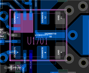
    About the layout of lm61460-q1,which pad can transfer the heat best?VIN,PGND or SW?We need to define which PIN get the larger PCB copper layer for best heat dissipation.
    In my opinion,VIN is the drain of the internal high side power MOSFET,and SW is the drain of the internal low side power MOSFET, they should share the more area in the chip die and has the best heat dissipation performace.Am I right?

  • Hi Zhiyuan,

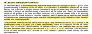
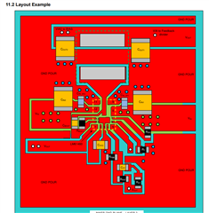
    If customers want to improve chip heat dissipation when drawing layout, they can refer to the suggestions in section 11.1.1 of the datasheet. VIN,PGND and SW all need good layout to improve thermal. Datasheet also provide a layout example. You can refer to this. Thanks a lot.

    Best Regards,

    Aurora