A related question is a question created from another question. When the related question is created, it will be automatically linked to the original question.
If you have a related question, please click the "Ask a related question" button in the top right corner. The newly created question will be automatically linked to this question.
We have a power supply product (input : 100~240Vac, output : 30V/2.34A) which used the design solution of TI UCC28780 + Navitas GaN MOSFET NV6115 + UCC24612, it can work well at full load 30V/2.34A, however, we are very surprised that there is about 5% failure rate when no loaded, most fail within the first hour and few fail happened within next 96 hours. We have made some tests and analysis as below for your reference, could you please help to analyse the cause and give us some better solution suggestion to solve this issue ? Please kindly let me know if you need any further information. Looking forward to your soon reply. Thank you in advance.
The higher input voltage, the more fail rate.
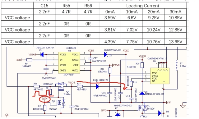
Regarding the failure units, see the detail failure description as attached, almost all of the top MOSFET ( U6 Navitas NV6115) is breakdown with 0Ω~570KΩ resistance, and some UCC28780 (U1) short-circuit damaged too. Please see the schematic and NV6115 datasheet as attached.
Please review the waveform videos between D & S of NV6115 at different condition ( no load 0mA /20mA/30mA), we can see that the DS waveform is more stable when loaded at 30mA. Perhaps some instant noise spike of UCC28780 at no load condition breakdown the MOSFET ?
We have verified that there is no fail after adding a absorption capacitor 47pF/1KV at DS of NV6115 and add a 30mA small load resistor at output too. If only add the capacitor or resistor, the fail is still existed, just the fail rate is lower. Moreover adding the resistor load at output can't meet the no load power requirement of energy efficient, so it's not the best option.
Thank you for using the UCC28780 in your application and for providing the schematic diagram of it.
Your failure analysis spreadsheet indicates basically 3 types of failures: a) failure of the upper GaN FET alone; b) failure of the GaN plus the BSS126, ACF controller, and additional parts; c) failure of the SR MOSFET alone.
The third type seems to be independent, but all are related somehow because the 47pF D-S cap and 30mA load appear to "solve" the problem. That means that the upper GaN FET is common to all of them. In (b), stresses from the GaN failure also overstress Q5 which fails and allows high voltage to damage U1 and Z5, and the high current burns out L7 and sometimes F1. Basically I think (b) and (a) are the same failure mode, with (b) having follow-on damage when (a) fails. Case (c) is not so easy to figure out, but I have a possibility which I will discuss later.
I will not pretend to know the answer, but I do have some suspicions and some concerns.
First, in the first video with load at 30mA, the stable frequency is about 25kHz which indicates operation in LPM. In the second video, load is 20mA and the frequency sometimes stays at 25kHz and sometimes goes lower. This indicates a transition from LPM to SBP. However this transition is not stable, which indicates that the FB current has some variation in it. In the third video at 0mA, we see that the frequency varies between 4000Hz and 2000Hz, which also indicates some variation of FB current. I'll get back to these points later.
About 3-4 years ago we had some experience with Navitas parts where they had some unreliable and unpredictable operation when their bias voltage at the VDD pin was below spec. The upper GaN FET relies on "bootstrapped" bias voltage through D2 to keep VCC high enough so it can keep VDD is spec so that the device can run reliably. During LPM and SBP, the upper GaN is not driven by PWMH, so reliable operation in this context means "do not switch".
I think that during LPM (~30mA load) the switching frequency is high enough (25kHz) to keep C15 charged up completely and U6 behaves correctly (does not switch). I think that during SBP (20mA and lower load), the switching frequency sometimes becomes too low to keep C15 charged up high enough and VDD on C14 droops out of spec. If VDD of U6 went to 0V, the GaN should be inert. But at some partial voltage (I don't know exactly what level) the GaN FET may lose control of itself and partially turn on due to noise or dv/dt or other reason. When U6 partially turns on, it has high voltage and current stress simultaneously and the peak power may damage the FET. This condition may result in failure quickly or after some long time. As I mentioned in the 3 types of failures above, sometimes only U6 fails, sometimes U6 fails in a way that damages other components with it.
My hypothesis for SR FET damage is this: Unwanted partial turn-on of U6 can also discharge the leakage energy stored in the clamp capacitors C26 and C27. This leakage energy builds up a voltage higher than the reflected output voltage. When U6 turn-on the higher clamp voltage can develop a high peak current that couples through the transformer and flows through the SR FET, peak current amplified by the turns ratio. Your SR FET is labeled AONS66540. I searched Alpha and Omega's website for this part and it does not show up. I did find AONS66520, AONS66521, and AONS66524, each of which becomes a smaller die size as the part number goes up. I am concerned that if the AONS66540 is a new unreleased device even smaller than the AONS66524, it may not have the capability to sustain the peak current that happens when U6 turns on. Or, it may be able to sustain it a few times, but not at higher repetition. One other possibility is that the current spike from U6 turn-on may generate a voltage spike > 150V across the SR-FET. These are the possibilities that I see might tie the SR-FET failures to U6.
I suggest that you try this following idea to prevent U6 from getting partial voltage at VCC and VDD: Try using a similar circuit as with U12 to drive Q3 when the frequency of RUN is > 24kHz, so that Q4 is always on when in LPM (when RUN is ~25kHz) and always off when RUN frequency is < 24kHz. Some hysteresis may be necessary. If this test circuit works on several boards, you may be able to find a way to simplify its function and accomplish the same goal: keep U6 fully off when in SBP mode.
Here are some other concerns that I have about your design, that may or may not have some influence on the U6-failure problem: 1. There is a circuit on the output that appears to be an over-current protection where Q1 is driven by U3 when CS1 voltage exceeds Verf1 voltage. a. Verf1 voltage looks like it is a function of the output voltage of U3. From the note at "Verf1" label, Verf1 = 0.0478V, but with 3.9K and 39K divider at R37 and R38, the LM321 output can only be as high as 0.526V. Maybe some resistor value is in error? b. Verf1 value depends on how high Vo of LM321 can get, which can very from board to board, so current limit may vary which may limit Iout < 2.34A. c. When Q1 is supposed to be off and LM321 off, Verf1 = 0V and any voltage on CS1 will make LM321 output go high and change Verf1. d. Full load voltage of CS1 is about 0.047V. LM321 has a typical input offset voltage of 2 mV and worst-case up to 9mV. So at light load, when CS1 < 9mV, it is possible that LM321 is always active and keeps Q1 on. The extra current through the optocoupler U2A from R23 might disturb the FB current at U1 and disturb regulation at light loads. This may be especially true if the load current puts CS1 voltage right at the offset voltage and LM321 turns on and off, disturbing the feedback loop. I suggest to derive Verf1 from a fixed voltage and add hysteresis to it. I also suggest to test your light-load operation with Q1 removed to see what effect it may be having on operation when Q1 is installed.
2. I am concerned about the inductor L6 in series with U6. Maybe this is only a ferrite bead, but I suggest to short it out temporarily to see if its inductance may have been adding voltage spikes to U6 and possibly overstressing it.
3. I suggest changing U4 from ISO7710F to ISO7730F. The -30F driver is pin compatible with the -10F, but the -30F uses edge-triggered drive from input-to-output whereas the -10F uses level-triggered drive. That means if INH starts to switch before VDD3 is in spec for some 50~80us, there may be only a partial pulse at PWMH instead of the full pulse width at INH. Using ISO7730F will prevent a partial PWMH to reach U6, and allow only full pulse widths. That will prevent U6 from turning off while it still has high peak current through it.
I know I put a lot of information here but please read the details carefully. Please remember that most of it is my "guess" at what might be happening, it is not certain. But I hope at least some of it can help you resolve the problem.
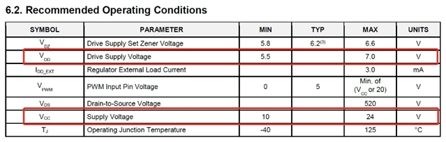
Many thanks for your detail analysis and suggestion on the possible reasons. Due to the products have already been produced a big qty, it's unrealistic to scracth them all, we hope can find a solution to resolve the upper MOSFET U6 breakdown issue by modify or change some components based on current PCB. We have done the test that change the values of C15, R55 and R56 to see if we can raise up the "Bootstrap" Voltage of C15 , in order to meet the requirement that the VCC of U6 can reach more than 10V, so that U6 can work under the specification condition. Here is the our test result for your reference. As you can see from the table, the VCC is still lower than 10V when the light load is below 20mA after adjusting the parameters. We think that the RUN pwm frequency of UCC28780 under SBP mode is too low, so it's unable to bootstrap the voltage. Do you have any more suggestions to increase the frequency of RUN, or how to modify the components or PCB to make C15 VCC reach more than 10V?
Thank you for your table of test results. I assume that the center row has one of R55 or R56 still populated, to be different from the bottom row.
In any case, I think it is probably more important that VDD be in spec than VCC, since VDD is derived from VCC through a regulator. The NV6115 does not state what the minimum drop-out voltage is for that regulator.
I understand that the best goal is to solve this problem by changing only existing component values. However, I think there is a chance that additional components not already on the board may be needed.
There is no way to increase the frequency of the RUN signal other than to increase the minimum load. However, RUN goes high at least 2us before any switching signal is sent from PWML or PWMH. In LPM and SBP modes, PWMH is not driven but the high-side device (NV6115) should be in spec so that it does not misbehave when the low-side switches.
To speed up the charging of high-side VCC and VDD, I suggest the following changes: a. Keep R55 and R56 = 0R. b. Reduce R19 value from 150R to 47R or lower. This will allow C14 and C17 to charge up faster. Except for the first pulse of each burst when in ABM, there is no reason to control the turn-on dv/dt of the high-side GaN because current from leakage inductance usually drives Vds down before PWMH goes high. c. Change C16 from 47pF to 10pF and R12 from 10R to 47R so that the PWM filter still has the same time constant but requires 1/5 the total charge to drive. d. With lower PWM charge, I think C17 can reduce from 22nF to 10nF. e. two ideas from the Navitas datasheet: - add 220kR across the Q4 FET to precharge C10 a little bit to help charge C15 faster, and - add diode across R19 to precharge C14 faster.
Please try these suggestions to see if they can help keep the bias of U6 in spec before PWML switches.
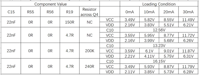
We tried to change some values and check the VCC and VDD per your suggestion, please see below table, it seems no much improvement when less than 20mA. If it's unable to resolve this issue by change some values of components, do you have any other suggestions by add some components or make some small modification on the circuit to resolve this issue ? Thank you again.
Thank you for the additional data. I am confused by the results shown in the last row. It seems that with 240R almost shorting out Q4, C10 voltage goes up as expected, but VCC and VDD are actually less than in the third row with 200K across Q4. That does not make sense to me. How are VCC and VDD voltages measured?
Did you try items (c) and (d) from my previous suggestions? Can you also try reducing C15 from 22nF to 10nF?
I don't have any more ideas for changing component values. I think a main contributor to the problem is that the low-side on-time is so short at light loads that the boot-strap charging of C15 is incomplete when the low-GaN FET turns off. If the light-load on-time can be made longer, C15 can charge higher.
But longer on-time means higher peak current which will drive the switching frequency down. It may also cause audible noise if the higher Ipk vibrates the magnetics at a frequency in the audible range.
Also how can the Ipk be increased for loads < 30mA? I think the PWMH signal can be used for this. PWMH is active during AAM and ABM and stops pulsing in LPM and SBP. So if a detector circuit sees that PWMH stops pulsing for >100us (for example) then the detector can trigger another circuit to divide the CS signal and raise the Ipk needed to meet the Vcst level. The same detector can remove the CS-divider when PWMH resumes at higher loads.
You can test this idea with a simple 2K resistor from CS to GND. This should double Ipk for light loads, but only test it with loads < 300mA! It also doubles Ipk for all loads, and this may cause trouble at high load. If the idea works, you can check for audible noise.