This thread has been locked.

If you have a related question, please click the "Ask a related question" button in the top right corner. The newly created question will be automatically linked to this question.

TPS51120: is not working only LDO part is only working, PWM is not being generated

Part Number: TPS51120

TPS51120.pdf

Hi,

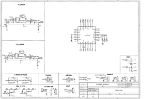
I am using TPS51120 for 3.3V and 5V generation, I tried both D-cap and current sense mode but, In my whole circuitry Just the VREG3,VREG5 and VREF2 is working none of the other part is working .the DRV pins are not even generating PWM , can anyone let me know what's wrong and help me out.

i have attached the schematics for the reference.

Thanks in advance.

  • The schematic is a little hard to follow, but check to make sure the jumpers for your enables are all in the right places to enable EN1 and EN2.

    Check the EN1 and EN2 voltage, as the internal pull-up current of 2μA could be pulled low by external leakage.  

    Also, the faults on the TPS51120 are all latching, so if the part is attempting to start-up, but experiencing a fault condition, it will stop and not attempt to restart until VIN is lowered below 2V. Monitor the LL1 and LL2 nets during initial start-up when the EN pin is first pulled high to look for some LL1 and LL2 pulses prior to shutdown.  If there are some pules, then they stop, the part is latrching offf.

  • hi peter

    thanks for your reply,

    the jumpers are properly put in place and all the pins have supply from V5Filt for enabling,

    i have captured the signals of LL .pulses are there and then it goes off.

    so what do you suggest ,what is exactly went  wrong.

  •  

    The TPS51120 is detecting a fault condition and shutting down.  Because the TPS51120 has latching faults, once the fault is detected, it stops switching and does not attempt to restart.

    I suspect that it's hitting over-current.  You have the CS1 and CS2 pins connected to the source of the low-side FET and also pulled up to V5Filt through a resistor.

    If R3/R10 are not installed, there is no path from the source of the low-side FET to GND, which is likely why you are seeing -2V on the switching node after the high-side FET turns off.

  • Hi Peter,

    I did remove the resistors R2,R5,R9 and Mounted R3,R10 and yet the system is entering fault mode.

  • Hi Sai,

    Peter is output of office this week. The schematic is too blurry and I could not read it. Could you send me the clear schematic to my email nancy_zhang@ti.com? I will review it. I will close this post since we will review offline.

    Thanks,

    Nancy

  • sure nancy you can close it here. I have sent you a mail.