This thread has been locked.

If you have a related question, please click the "Ask a related question" button in the top right corner. The newly created question will be automatically linked to this question.

LP38692-ADJ: Layout Review

Part Number: LP38692-ADJ

Hi Team,

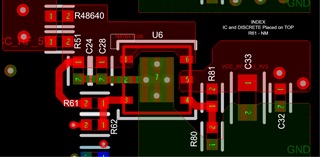
We are using the LP38692SD-ADJ/NOPB LDO part in our Layout Board file. I had attached the images of the Board file and Schematics. Please review the layout and share your feedback with us.

The PCB we are using is of 12 Layers:

IC - Place on top

Layers 2,4,9 and 11 are Ground

Enable Signal is from L5

Thanks and regards

- Teja.

  • Hi Teja, 

    I looked at the schematics and layout portion that was shared.

    Can you share the application for this device? This is an older LDO and we might have a better device with the given conditions. 

    Is there a reason to have two 0Ohms resistors in parallel at the input? it is common to see a 0Ohm jumper but I was curious to see why there are two in parallel. 

    This device does not have an active pull down on the EN pin, therefore, please make sure that the signal that drives EN does not go below GND level or higher than Vin. A pulldown resistor can be installed. 

    Be aware that there are some scenarios where reverse current can occur: 

    Layout looks ok, my biggest comment is that perhaps a newer LDO might provide a cleaner Layout since In and out tend to be on opposite sides with newer WSON packages. 

    This allows for better GND on the top, but overall it follows the recommended layout from the Data Sheet:

    Here is a quick suggestion: TPS746 data sheet, product information and support | TI.com

    Best, 

    Edgar Acosta

  • Hi Edgar Acosta,

    Thanks for your Valuable feedback.

    • The application of the device is quite as same as the LDO we need to convert 5.5V to 3.3V. This part is is meeting our requirement. The reason behind not using the new part is as of we had drafted the schematics and layout also done as we need to meet our deadlines we are proceeding with the same part LP38692SD-ADJ/NOPB. Thanks for the suggestion of the new part we will take this into consideration for the future recommendations. 
    • The reason for the two parallel 0 ohms is for the debugging purpose, we can isolate. the reason for two parallel resistors is for the BOM optimization as the res is of 1A we had added two resistors for better reliability. 
    • The EN pin of the device ahs the pull down on the other end, i hope that's fine. Please correct me if i am wrong.
    • The thermal vias also implemented as mentioned in the above image.

    Thanks and regards,

    - Teja

  • Hi Teja, 

    Thank you for the comments and information. 

    Is the pull down is on the other end, then I do not see a problem with this. 

    As for the thermal vias, it is highly suggested to place as many as possible. This will depend on the capabilities of the fabricator. 

    Other than this, everything looks good. 

    Best, 

    Edgar Acosta

  • Hi Teja, 

    Thank you for sharing such information. 

    As for the thermal vias, it is recommended to place as many as possible to help improve thermal performance. 

    Other than this, everything looks good. No further comments. 

    Best, 

    Edgar Acosta