This thread has been locked.

If you have a related question, please click the "Ask a related question" button in the top right corner. The newly created question will be automatically linked to this question.

TPS61288: TPS61288 design

Part Number: TPS61288
Other Parts Discussed in Thread: TPS552892, ,

Hi,Fergus:

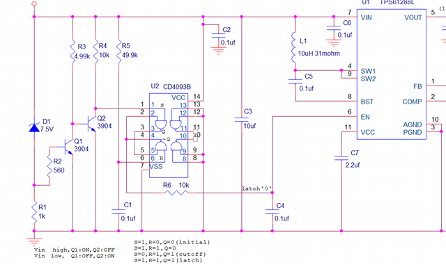
I see a light of solving the Issue. The clamp circuit doesn’t have enough drive ability to drive Q3.

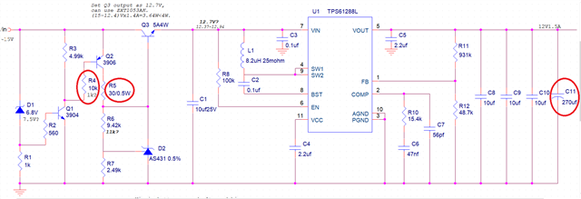
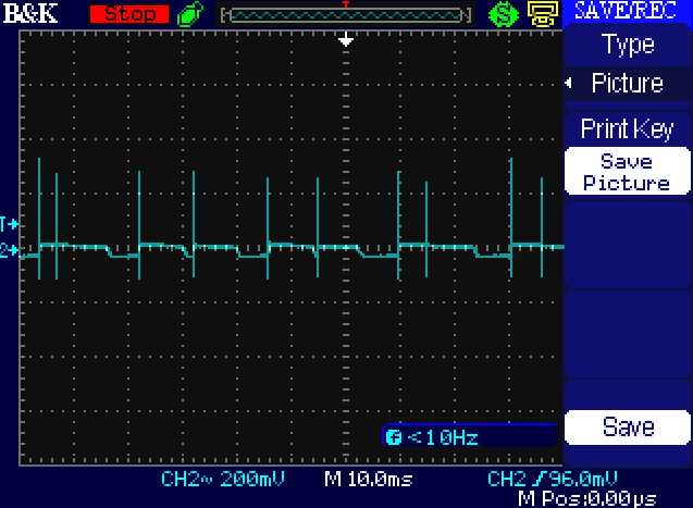
I add a 10ohm resistor on AS431 cathode and reduce the serial resistor R5 from 300ohm to 100ohm. The voltage cross 10ohm only 49mV@Vin=15V, and 0.2mV@Vin=7.4V.

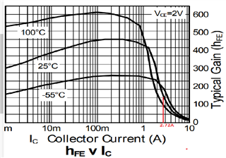
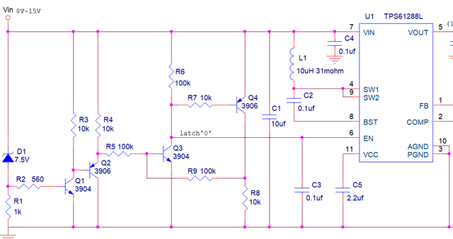
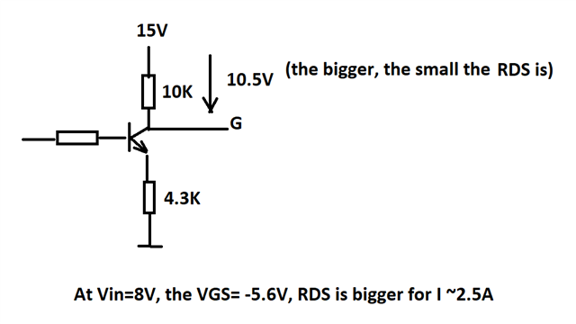
I use a PNP transistor to amplify the output current, see attachment. It works when Vin=9.5V~15V. still have issue at low end, because the current flowing Q3 is bigger and low Vin  can't provide enough output current. 

The next step: I will use a Darlington PNP to get bigger current gain, hope it will work.

I though to move the clamp circuit at output side, Because Vout is >12V, it's easy to handle parameters. and use EN pin to cut-off when Vin < 8V. However I don't know the details of customer side LED drive circuit. It has risk when project released, it has issues. 

Would you please give your suggestion for my modified schematic.

Thanks.

Chang

8V~15V inut--12V1.2Aoutput.pdf

  • Hi Chang,

    For the Darlington PNP, I consider it is useless because the Q3 base current is mainly from Q2, with will be (Vin-12V-Vbe)/100, maybe 30mA max.

    you can change R5 to a smaller value to ensure enough Q3 base current.

    Another Potential problem, the loop may conflict between the two stages. 

    I have a better choice for you, you can use a buck-boost device, like TPS552892, it will increase efficiency and reduce outside devices.

    Also, TPS552892 has an output current control ,which is suit for LED driver.

    please see the website.

    TPS552892 data sheet, product information and support | TI.com

    Best Regards

    Fergus

  • Hi, Fergus:

    I think a very simple way to solve Q3 drive issue. AS431 circuit just provides a clamped voltage 12V at Q3 output when Vin>12V.  When Vin drops below 12V, The As431 circuit is not in normal condition, just pass Vin to its output. It does not have enough voltage to increase its output current.

    Now I am thinking: the AS431 Vout is tied to Q3 output for clamping. the Q3 base bias current can be acquired from Vin by added a bias resistor. my preliminary calculation is 49.9 ohm 0.5W.

    On Monday I work at home. On Tuesday I will go to lab to do the test. Hope it will be ok.

    Thank you very much.

    Chang

  • Hi Chang,

    The AS431 has a maximum cathode Current Range -100mA to 150mA, it cannot clamp the power 12V.

    It is recommended to clamp the base to be 12V and enlarge the bias current from Vin.

    Also, I think the bias resistor 0.5W power is too large.

    What do you think of the usage of TPS552892?

    Best Regards

    Fergus

  • Fergus:

    • AS431 does clamps voltage output to 12V. Because AS431 voltage output is tied to Q3 base, the Q3 emitter output will be 12V-Vbe (so I set the AS431 output 12.7V). Q3 output current is determined by its base current, which is determined by the voltage cross R5 and R5 value. Problem is when the Vin is below 12V, voltage cross R5 is only about 0.7~0.8V. current flowing R5 = AS431 reference current + cathode current + Q3 base current. It is difficult to handle. 
    • I consider adding a bias resistor between Q3 base and Vin, it will invalidate cut-off function. The cut-off function will limit the current flowing Q3 (now the max current is 12Vx1.02 x1.4A(max) /0.9 (efficiency)/7V(cutoff voltage)=2.72A. I check Q3 (ZXT1053AK) datesheet, the gain is 100 at 100 degree and 150 at 25 degree. 
    • , take gain=100, Q3 base current(max)=2.72A/100=27mA. so R5=0.8V/27mA=30ohm. When Vin=15V, current flowing R5=(15V-12V)/30 ohm=0.1A, consume 0.1Ax3V=0.3W.
    • The buck-boost chip is a good choice, but the cost is high.(~$4). The potential customer may place an 250K order, the target BOM cost is $2.50. I will try my best to work on my current design, but if it doesn't work, I will ask our Sales Department to negotiate with customer.
    • Thanks. really appreciate your help.
    • Chang 
  • Another consideration just raises up. the AS431 work normally, when Vin >12V and output 12V. It just passes Vin out when Vin <12V. I don't know if there is a dead point (voltage cross R5=0). tomorrow when I go to office, I will try to find it out.

    Anyway if it doesn't work, I will move the clamp circuit to TPS61288 output side, As long I set TPS61288 output 13V, the AS431 circuit always in normal stage. It will much easy. In this case, I will use TPS61288 EN pin as cutoff. What is the lowest voltage on EN pin to disable TPS61288? can I just use a zener and a resistor on EN pin?

    Thanks.

    Chang

  • Hi Chang,

    1. when TPS61288's input is close to its output, like 12.3Vin and 13Vout, it will trigger its minimum duty and it will cause large output ripple.

    I remember you mentioned this question before. Usually, it is not recommended to work in this condition, but it is OK anyway.

    What I'd like to remind you is that in former design Vin=12 and Vo=12V, it may enter minimum duty condition, possibly.

    that is, when Vin is above 12V, the whole ripple may be very large.

    2. for EN pin, you can just use two resistors to divide the input voltage, the high-level threshold is 1.2V and the pin's max voltage is 6V, it will be enough.

    3.Move the clamp circuit to output is feasible. But due to its always working, the thermal may be bad according to the input condition.

    In this application, when Vin is above about 13V, the device will completely shut down and no switching, it is better than former circuit structure in output ripple.

    3. I think Q3 is not full saturation conduction when Vin <12V.

    Problem is when the Vin is below 12V, voltage cross R5 is only about 0.7~0.8V.

    why is that? I think the voltage cross R5 is nearly 0 if Vin is below 12V.

    When Vin is 11V, Q1 and Q2 are saturation conduction, AS431 is not able to output current to rise the base voltage to be 12V, it can only keep base voltage 11V, base voltage is not 0.7V higher than emitter, Q3 cannot be saturate conduction.

    4. TPS552892 can be cheaper, please connect our FAE or sales.

    Best Regards

    Fergus

  • Fergus:

    Q3 drive ability is solved by changing R5 to 30 ohm/0.5W. Now for Vin varies between7.4V~15V, output is 11.81V~11.84V@load 1.2A. The maximum ripple p-p is 200mV by adding an 270uF aluminum cap (16SVPG270M, without it, ripple 1V).

    Still has some issues: Audible noise happens at cutoff point (around Vin=7.4V) and transient point (around 13V). Vin >13.5V, audible noise disappears.

    The root cause of cutoof point noise is Q1 changes its status from ON to OFF not steep(take long time). I may try below 2 methods:

    1. Shunt a cap with R1.

    2. use a comparator to replace Q1.

    I don't know how to solve the TPS61288 transient point noise (around Vin 13V), probably also the drive ability (when Vin is near the stabilized voltage, voltage cross R5 is small, even 0, no current gain.

    Thanks.

    Chang

  • It seems not the drive ability issue at ~13V.  Vin=13.3V, Iin=1.24A, quiet; Vin=13.4V, Iin=1.24A, audible noise starts; Vin=14.1V, Iin=1.24A, noise disappears.

  • Vin= 13V~15V, the audible noise happens in the bypass stage, because the current is 1.24A. But higher than 14.1V, no noise. input current reaches its maximum at 7V which is 2.85A

  • Hi Chang,

    please separate the two issues, one is that when Vin is close to AS431 target, and the other is Vin of TPS61288 is close to TPS61288 output target.

    The two issue both can lead to noise problem.

    you can change AS431 target to see which issue will cause the noise.

    for Vin is close to AS431 target, it may cause by drive ability as you said, but I doubt that drive ability will reduce with the input voltage, as I mentioned before.

    I think the voltage cross R5 is nearly 0 if Vin is below 12V

    for Vin of TPS61288 is close to TPS61288 output target, you can check the inductor current or SW waveforms to see if there is audible noise.

    if this is the noise source, you can remove some output capacitance to increase the frequency. Once the frequency is higher than 20kHz, the noise will disappear. but there is still possibility when the load is light, the frequency will decrease again.

    At last, I recommend using a buck-boost scheme or you can just choose a cheap buck device to make a second stage, it will be much easier.

    Best Regards

    Fergus


  • Hi, Fergus:

    Thank you very much. 

    So the output capacitance determines the switching frequency. To reduce the big ripple at 12V, I add a 270uf aluminum cap (reduce ripple from 1V to 200mV), this may be the root cause of noise at high input voltage. I may try 100uf or 47uf (customer LED drive spec. is ripple <500mV)

    Once again, thank you very much.

    Chang

    PS: the cutoff function may cause hiccup, when battery voltage is low than 7.4V, it cuts off the battery input -> battery voltage will rise -> turn on circuit again....... I am consider adding a one-shot circuit.

  • sorry, the frequency your mentioned is ripple frequency which is related audible noise. I will try the compromise of ripple < 500mV and no audible noise.

    Thanks .

  • Hi Chang,

    It's pleasure to help.

    please check if there will be noise when the load is lighter.

    It is always complex to deal with noise problem.

    Best Regards

    Fergus

  • Hi, Fergus:

    I think you guide me to the right track. For high end of the Vin, I change the aluminum cap value from 270uf to 100uf(plus 40uf ceramic caps) , almost no audible noise. Only at Vin=14.3V has very light audible noise. The maximum ripple is 520mV (20mV larger than customer spec.). I add a 1uH2A inductor and 10uf cap filter, the ripple almost disappeared, only at rising edge has overshoot 520mV. I will try other inductor with large DC resistor to see the results.

    For the low end of Vin, I need to make the cutoff time short (make transition quickly), and add a latch circuit that circuit remains cutoff when battery voltage goes up. I decide to use digital circuit to implement it. In analog circuit the impedance is not easy to control and caused much trouble (drive ability, transistor state transition) drive me crazy, especially in the condition of varying Vin.

    Below is my plan for low end Vin circuit.  

    Thanks.

    Chang

  • Hi, Fergus:

    I think Vin high end ripple noise issue is solved. By adding a 2.2uH 0.081ohm DCR L and 10uf C filter at output, at Vin=14.1V the output ripple is 300mV (compare 520mV with 1uf 0.051ohm DCR), and noise is barely noticeable. although the noise frequency is still in human ear range, but the noise energy is small. The total output cap is only 70uf (probably I can further reduce the cap).

    I will work on low end issue. first I need to purchase parts. it may take several days. I will close this help ticket. If I meet new problem I will issue new ticket.

    Thank you very much. Your are real helpful.

    Chang

  • Hi Chang,

    It is my pleasure to help.

    Best Regards

    Fergus

  • Hi, Fergus:

    I have trouble to use EN pin for battery cutoff and latch. I have 2 cutoff/latch circuits, both works if I don't connect to TPS61288 circuit EN pin. see below schematic.

    cutofff/latch circuit 1:

    cutofff/latch circuit 2:

    Both circuit output Vin to EN pin when Vin high, and output 0.000V (circuit 1)/output 0.24V (circuit 2). I check the datasheet , EN low is 0.4V.

    When I connect the cutoff/latch circuit to TPS61288, it doesn't cutoff, the input current drops from 2.1A to 0.98A.

    I purchase a TPS61288EVM-064 board, and set the jumper to EN->GND, same results: TPS 61288 still output voltage but current drops.

    Please help.

    Thanks.

    Chang

  • Correction:

    Both circuit output Vin to EN pin when Vin high, and output 0.000V (circuit 1)/output 0.24V (circuit 2) WHEN VIN LOW.

    TPS61288VEM-064 User Guide link:

     https://www.ti.com/lit/ug/slvubw6a/slvubw6a.pdf?ts=1685485502544&ref_url=https%253A%252F%252Fwww.ti.com%252Ftool%252FTPS61288EVM-064

    schematic is on page 3. 

  • Hi Chang,

    As you can see, TPS61288 is shutdown when EN is low, but the device cannot isolate output from input.

    The body diode of the higher MOSFET is automatically on and current can flow through it to the load.

    If the load disconnection is needed, Buck-Boost will be your best choice. Or you need to add an iso-FET. 

    I think a hysteresis comparator will be simpler and more accurate than TVS and transistors.

    Best Regards

    Fergus

  • Hi, Fergus:

    Would you please teach me how to use a hysteresis comparator to disconnect the load?

    Thanks.

    Chang

  • Yesterday I purchased a P-channel enhancement type MOSFET SSM3J332R (30V 6A 1W) for cut the load, and overnight delivery this morning.

    But I am worrying about this MOSFET may be not good for our application. 

    1. The package is too small, SOT-23, Although its RDS(on) = 50mohom ~100mohm. for a 2.5A current, its max voltage drop is 2.5A  x 100mohm = 0.25V and  the max power consumption is 2.5A x 0.25V = 0.625W.

    2. The TPS61288 has inductor and caps. Will 30V and 6A be enough for current and voltage surge?

    Thanks.

    Chang

  • Hi Chang,

    Sorry for the confusing.

    The hysteresis comparator can be used to replace the TVS and CD4091 circuit.

    For your P-MOS, it looks it will be enough for the voltage and current expect the gate voltage.

    its gate voltage is +-12V, so it will be over range to connect the gate to GND as the source voltage will be 15V max.

    Best Regards

    Fergus

  • <its gate voltage is +-12V, so it will be over range to connect the gate to GND as the source voltage will be 15V max.>

    Yes I consider this and have a drive circuit as below.

  • Hi Chang,

    It looks ok with the circuit.

    When Vin is low, the MOS will be hot, please take care of the heat dissipation.

    Also, the surge current will occur at start up period and load dynamic.

    Please arrange the start/shutdown sequency to ensure the MOS fully condition to avoid large power loss.

    Best Regards

    Fergus

  • I think TPS61288 has soft-start implemented. And on TPS input side I only put a 10uf cap. Although the switching choke is at input side, its surge will be limited by the soft-start. However, I am still not confident with the small package of MOSFET (I should buy TO-252 package with 15A). Let's see in a couple of hours (I will receive the MOSFET). Look at TPS61288, such a small package can conduct 18A current, I feel a little bit relieved.

    Load dynamic: the real load is LCD backlight (12V1.2A, max 1.4A). I think the backlight is always connected. I use 10 ohm power resistors as load. The backlight drive circuit may cause some surge (customer spec. says 5A inrush current).

    Before the inrush current can be absorbed by TPS61288. Now I move AS431 clamp circuit from input side to output side for avoiding low drive voltage/current dilemma. The NPN transistor ZXT1053AK is only rated 5A4W, hope the surge is momentary, ZXT1053AK can stand this surge. Otherwise I will re-choose the NPN. the test results is good (except the cut-off/latch function). see below new schematic and test results. 

    schematic 5-31-2023.pdf2541.test results.docx

    Thanks.

  • Hi Chang,

    You mentioned that you have the NPN transistor at outside, so it can be an isolation between input and output.

    one of the input P-FET and outside NPN will be enough.

    You could have a comprehensive testing after everything is done.

    It will be safe to have a thermal result after all.

    Best Regards

    Fergus 

  • Hi, Fergus:

    For some reason, I didn't receive the P MOSFET yesterday and couldn't test it.

    Yesterday I sent you a blank schematic, I don't why. resending....

    In the new schematic, I move the AS431 to the output side. You can see how tough the AS431 drive voltage/current is. consider the component tolerance, prototype working doesn't mean mass production ok. I calculate the worst case of AS431 Vout and TPS61288 Vout. in the worst case, the drive current is only 7mA (very marginal) and I raise the TPS61288 Vout to 12.53V

    In this schematic, the cutoff/latch is connected to EN pin. I will use PMOS at input side.

    5584.schematic 5-31-2023.pdf

    Thanks.

    Chang

  • Hi Chang,

    Will 12.53V be enough?

    the base voltage will be 12.5 as the 431 ref is 2.5V, and the base current will be (12.53-12.5)/30=1mA, voltage deviation not considered. 

    The power loss could be a potential problem.

    Actually, the circuit is a little too complicated, I have to say.

    Best Regards

    Fergus

  • Hi, Fergus:

    Sorry, a tyro, I set to 13.53V.

    yesterday, I added PMOS. The PMOS is ok. but because of the PMOS voltage drop (0.3V), at Vin=9V, the input current is big than previous test results. and audible noise happens, input current drops. I check the circuit; the drive resistor is 50 ohm not 30 ohm.  I will change to 30 ohm to test. I look at ZXT1053AK datasheet again (the gain versus temperature), at high temperature the gain drops. Probably I need to find another transistor.

    Thanks.

    Chang

  • Something is wrong, probably not the drive ability issue. now the AS431 clamp circuit is on the output side (unlike the clamp circuit on the input side, which provides the current). If the load current reduced, it won't affect TPS61288. the audible noise is caused by adding the cutoff/latch circuit. without the cutoff/latch circuit, it works fine (as the test results shows).

  • It does affect TPS61288 working, because Vout drops too

  • Find the problem. P MOS can't conduct heavy current. When load is 12 ohm (~1A). Vds is 0.25mV. Wnen load is 6 ohm, it should be ~2A. I got 1.15A and Vds=5V, not saturated.

  • Hi, Fergus:

    The small MOSFET has RDS=100~150 mohm, and at low Vin, the current is bigger. The RDS will increase if VGS is small which at low Vin it is small.

    Now I select Si4155DY-T1-GE3 whose RDS is 15 mohm, but Cgs is large (~1000pf)) my drive circuit is:

    Please kind check if anything I neglect.

  • Hi cao:

      Fergus is out of office from 5th to 6th , will reply you after back, thanks.

  • Hi, Fergus:

    fix the issue by moving the VGS voltage divider lower resistor from NPN emitter to collector. so the emitter tied to GND and the voltage divider between Vin and collector.

    Now I have a fully functional prototype.

    Thank you for your help.

    Chang

  • Hi Chang,

    Glad you have a complete design.

    Wish everything goes well with you.

    Best Regards

    Fergus

  • Thank for your help in the past one month.

    Chang