This thread has been locked.

If you have a related question, please click the "Ask a related question" button in the top right corner. The newly created question will be automatically linked to this question.

UCC27531-Q1: +18V and -5V output gate driver for SiC Mosfet

Part Number: UCC27531-Q1
Other Parts Discussed in Thread: UCC27614, UCC23513, UCC27532-Q1, UCC27624-Q1

Hi,

I am looking to drive the SiC Mosfet requiring -5V and 18V Vgs.

Also the sink current is 2.81A and source current is 2.56.

If I am not wrong, I can use this IC for the purpose, but IC source current is 2.5A. Do you have any IC with higher source current? Or do you think I can use the same IC for the purpose?

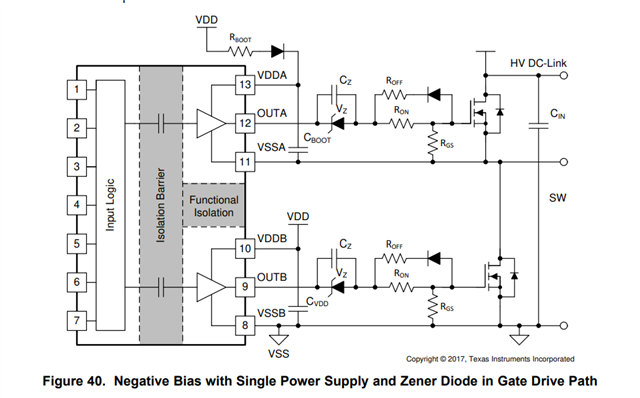
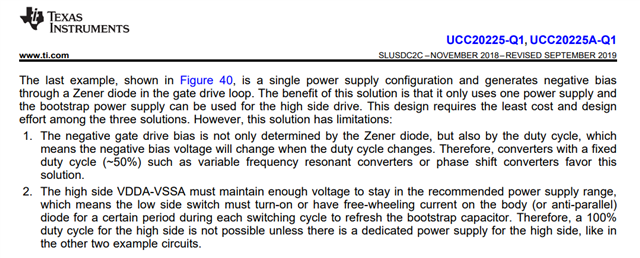
Also for driving at -5V, I am taking the following circuit as reference.

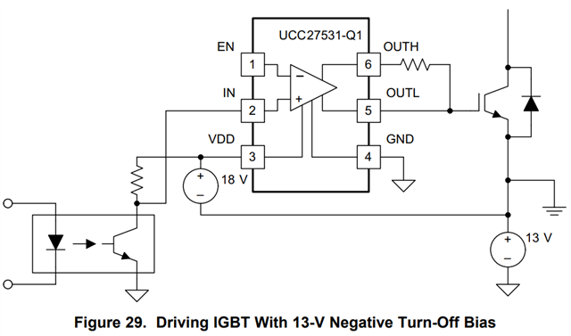
For this purpose, I will replace the 13V with a 5V supply but I do not understand the purpose of optocoupler at VDD?

  • Hello Alina,

    This looks like it should work. Assuming you need Q1 rating, another option is UCC27532-Q1, it has 5A sink so it can meet that current requirement. Both fall slightly short of the 2.56A source, but it is very close. If Q1 is not required, there are more options like UCC27614.

    The optocouple is helping to ensure the IN signal is okay relative to VDD/GND. It also gives isolation. The connection to VDD is just the pull-up for the Rx of the optocouple. Depending on how you set up the grounds, IN may be okay directly connected to a controller, or require only a normal level-shift circuit. 

    Here is another circuit that can be used for negative bias with only 1 supply. It has some drawbacks such as duty-cycle dependency and can only hold negative for a certain amount of time. I just wanted to share in case it works for your application.

    Thanks,

    Alex M.

  • Hi, thank you for the response. What limitations can I have with the duty cycle for one supply option?

  • Hi Alina,

    Sorry, I should have included my source for the image. It is from the UCC20225-Q1 datasheet in this case:

    There are some other options shown in this datasheet as well. It is for an isolated driver, but these solutions should work just as well for non-isolated.

    Thanks,

    Alex M.

  • Thank Alex, for UCC27614 can I use the same negative supply approach for +18 and -5V on the output? In the datasheet, there is no example circuit.

  • Hi Alina,

    Yes, you can use that method with UCC27614. It is possible to use that method with essentially any driver. It is basically taking the driver output, and shifting it down for the gate. To the driver, there is no difference.

    Thanks,

    Alex M.

  • Thanks, can you suggest how to select the optocoupler to isolate my PWM. The PWM is 200kHz. 

  • Hi Alina,

    As far as I am aware, TI does not sell optocouplers. However, we have isolators such as ISO7710 that fulfill a similar role. You could ask this question to the Isolators group. 

    However, I still think this design may not require an optocoupler. As long as the controller is connected to the same ground as the driver, it will be able to work. There may be issues with noise/ground loops that motivate this isolation, but I think it is possible to avoid using it. 

    Thanks,

    Alex M.

  • Hi Alex,

    I have a 4 pin SiC Mosfet. So what I understand is that my kelvin pin will be connected to the common of 18V and -5V while the source will be connected with the ground of the IC/dricver/battery since it is non isolated.

    I have done a simulation with a different driver. 

    I want to use the same concept with the TI driver. The concept will be like this?

    Also, can you suggest an IC that can generate 18V and -5V in a single package? I wanted to uses UCC14141_Q1 but it is not in stock by TI?

  • Hello Alina,

    Is it okay for the kelvin and source pin to be at a different potential? Isn't there a near short across the 5V supply?

    As for the bias, one option is a split rail buck-boost like these. I only see options up to +15V though. A charge pump IC could be used for the -5V, but I don't see any that support a split rail and +15V. I think it should be possible to use a normal, ground referenced positive supply and a separate negative supply.

    To generate both at once, a transformer-based topology is probably the easiest way. There are isolated DC/DC controllers, as well as modules that integrate the transformer. I am not aware of any other modules like UCC14141 that generate the negative rail so easily though.

    Thanks,

    Alex M.

  • Hi Alexander, that is exactly what I am trying to understand. Where to connect my kelvin source and supply ground.

    I tried another simulation with this configuration. In this sense then my -5 and 18V needs to be an isolated supply compared to my main circuit. So I will connect my kelvin source and battery negative together, where as my -5V and 18V will be isolated with island ground?
    Also, then my PWM is generated using the same battery negative. So I can isolate it as well on the input and use an isolated gate driver or it should work on a non isolated gate driver as well?

    For isolated gate driver, I have been looking at UCC23513_Q1.

  • Hi Alina,

    Okay, I think I understand better now. I had been treating the 0V as the IC's ground instead of the battery ground. I adjusted my simulation also and I see the IN issue (assuming PWM is generated on battery negative like you say). 

    Basically, I think you need some sort of level shift. You could achieve that through isolation, or other methods (since its only off by 5V). There may be other requirements for your system to use isolation here though. Also, depending on the voltage levels, it may be possible to use a CMOS driver like UCC27532-Q1. It's thresholds are nominally 9.4V, so if you have a 5-10V signal, it may work with no level shifting. 

    If you do decide to use isolation, It would probably be more cost-effective to use an isolated gate driver. I can send this thread to someone from that team if you have questions about that. 

    As for the Kelvin pin, I'm not sure you can take full advantage of it with this setup. To me, the point of that pin is to have a low L gate drive loop by connecting directly to the driver GND. But I'm not sure that is possible here.

    Thanks,

    Alex M. 

  • I think I need to use an isolated supply for the gate driver and the pwm needs to be isolated as well then. I think it will be easier to use an isolated driver in that case rather than looking for ways to isolate my PWM with this circuit?

    My source and sink current requirement has gone fairly high and I am looking for +/-10A source and sink current now.

    My application is a non-isolated buck converter. It is an asynchronous topology. So all my ground are the same as battery negative including my PWM IC and auxilary supply. 

  • Hi Alina,

    The highest drive current non-isolated device we have right now is UCC27614 (10A, not automotive), or paralleled UCC27624-Q1 (2x5A, basically the same thing). 

    Generally, you can find higher drive currents on isolated drivers, so that sounds like it may be the best fit here. I will send this thread to a member of our isolated gate drivers team for further comments/recommendations.

    Thanks,

    Alex M.

  • Hi Alina,

    You can use our UCC53X0 family, which ranges up to 10A output current for the 5390 version. You can use an isolated supply, but you can also use a bootstrap supply for a buck converter.

    Best regards,

    Sean

  • Hi Sean and Alexander,

    I have finalized my driver. I will use a non-isolated gate driver UCC27511AQDBVRQ1. I have sorted out my ground issue. I am in the schematic phase. Thank you so much for your support. It helped me a lot. I am resolving he issue and will create a new one if needed in future.